In short, Artificial Intelligence (AI) is being integrated into Plasma-Enhanced Chemical Vapor Deposition (PECVD) to automate and optimize the complex task of process control. By analyzing vast amounts of experimental data, AI models can predict how changes in process parameters—like temperature, pressure, and gas flow—will affect the final thin film properties. This allows researchers and manufacturers to find the ideal "recipe" for a specific application much faster and more cost-effectively than through traditional trial-and-error methods.
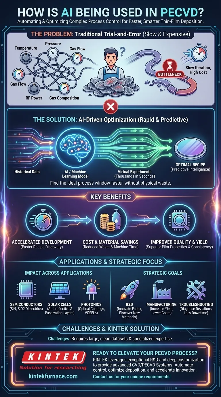
The core challenge in PECVD is its complexity; dozens of variables interact to determine the quality of the final product. AI transforms this challenge by enabling a shift from slow, expensive physical experimentation to rapid, data-driven virtual optimization, significantly accelerating material discovery and improving manufacturing yield.
The Core Challenge: Why PECVD Optimization is So Difficult
PECVD is a cornerstone of modern fabrication, used to create the microscopic thin films that power everything from semiconductors to solar cells. However, achieving the perfect film is notoriously difficult.
The Problem of "Recipe" Development
A PECVD process is defined by its "recipe"—a precise set of input parameters. These include substrate temperature, chamber pressure, gas flow rates, gas composition, RF power, and frequency.
Even a minor change in one parameter can have a significant and often unpredictable effect on the final film's properties, such as its thickness, uniformity, refractive index, and internal stress.
The High Cost of Trial-and-Error
Traditionally, developing a new PECVD recipe is a manual, iterative process. Engineers run dozens or even hundreds of experiments, tweaking one variable at a time to observe its effect.
This approach is extremely slow, consumes expensive materials and gases, and requires significant machine time and engineering resources. It is a major bottleneck in both research and production environments.
How AI Provides a Solution
AI, and specifically machine learning (ML), provides a powerful new toolkit for navigating the complexity of PECVD process control. It replaces guesswork and slow iteration with predictive intelligence.
Building Predictive Models
AI systems are trained on historical data from past PECVD runs. The model learns the intricate, non-linear relationships between the dozens of input parameters and the resulting film quality metrics.
Once trained, this model can instantly predict the outcome of a given recipe without needing to run a physical experiment.
Enabling Virtual Experimentation
With a predictive model, engineers can run thousands of "virtual experiments" in seconds. They can explore the entire process window on a computer, identifying promising recipes for specific goals.
This dramatically reduces the number of physical experiments required, saving immense amounts of time, money, and materials. The AI guides engineers directly to the most promising sets of parameters to test in the real world.
Enhancing Quality and Yield
By finding the true optimal process window, AI helps create films with superior properties and consistency. In a high-volume manufacturing setting, this leads to higher device yields, less scrap, and more reliable end products. This is critical for applications like semiconductors, LEDs, and MEMS devices.
The Impact Across Key Applications
The benefits of AI-driven optimization are being realized across the full spectrum of PECVD applications.
Semiconductors and Electronics
In semiconductor fabrication, PECVD is used to deposit critical dielectric and passivation layers like silicon nitride (SiN) and silicon dioxide (SiO2). AI helps achieve the precise thickness, uniformity, and low defect density required for high-performance integrated circuits.
Solar Cell Manufacturing
For solar cells, AI optimizes the deposition of anti-reflective and passivation layers. This directly enhances the cell's efficiency by maximizing light absorption and minimizing energy loss, contributing to more powerful and cost-effective solar energy.
Photonics and Optical Coatings
In applications like high-brightness LEDs, VCSELs, and custom optical filters, the exact refractive index and thickness of the deposited film are critical. AI enables the precise control needed to manufacture these components with high reliability and performance.
Understanding the Trade-offs
Integrating AI is not a magic bullet and comes with its own set of challenges.
The Data Requirement
Machine learning models are only as good as the data they are trained on. Effective AI integration requires a large, clean, and well-structured dataset of past experimental runs. Companies without robust data collection practices may struggle to implement it.
Initial Implementation Complexity
Building and deploying an AI model for process control requires specialized expertise in both data science and materials science. It represents an upfront investment in talent and infrastructure that may be a barrier for smaller operations.
Making the Right Choice for Your Goal
Adopting AI for PECVD is a strategic decision that depends on your primary objectives.
- If your primary focus is Research & Development: AI dramatically accelerates the discovery of new material properties and process windows, allowing you to innovate faster.
- If your primary focus is High-Volume Manufacturing: AI is a powerful tool for improving process stability, increasing yield, and reducing operational costs.
- If your primary focus is Process Troubleshooting: An AI model can quickly diagnose process deviations and suggest corrective actions, minimizing downtime and scrap.
Ultimately, integrating AI allows you to move beyond intuition-based engineering and toward a more precise, predictable, and data-driven approach to thin-film deposition.
Summary Table:
| Aspect | AI Application in PECVD |
|---|---|
| Process Optimization | Predicts effects of parameters like temperature and pressure on film properties. |
| Efficiency Gains | Reduces trial-and-error experiments, saving time and costs. |
| Key Benefits | Faster recipe development, improved yield, and enhanced film quality. |
| Applications | Semiconductors, solar cells, photonics, and optical coatings. |
Ready to elevate your PECVD processes with AI-driven solutions? KINTEK leverages exceptional R&D and in-house manufacturing to provide advanced high-temperature furnace solutions, including our specialized CVD/PECVD Systems. Our strong deep customization capability ensures we can precisely meet your unique experimental requirements, helping you automate process control, optimize thin-film deposition, and accelerate innovation. Contact us today to discuss how we can support your goals in research, manufacturing, or process troubleshooting!
Visual Guide
Related Products
- Slide PECVD Tube Furnace with Liquid Gasifier PECVD Machine
- RF PECVD System Radio Frequency Plasma Enhanced Chemical Vapor Deposition
- Inclined Rotary Plasma Enhanced Chemical Deposition PECVD Tube Furnace Machine
- Inclined Rotary Plasma Enhanced Chemical Deposition PECVD Tube Furnace Machine
- Multi Heating Zones CVD Tube Furnace Machine for Chemical Vapor Deposition Equipment
People Also Ask
- What plasma source is used in PE-CVD tube furnaces? Unlock Low-Temperature, High-Quality Deposition
- In which industries is the tube furnace commonly used? Essential for Materials Science, Energy, and More
- How does PECVD equipment contribute to TOPCon bottom cells? Mastering Hydrogenation for Maximum Solar Efficiency
- What are the main advantages of PECVD tube furnaces compared to CVD tube furnaces? Lower Temp, Faster Deposition, and More
- How does a hydrogen reduction environment in an industrial tube furnace facilitate gold-copper alloy microspheres?


