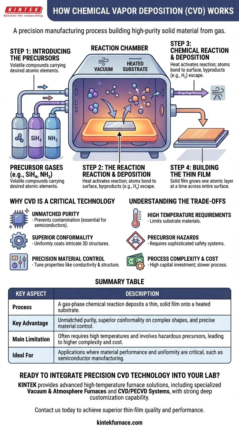
At its core, Chemical Vapor Deposition (CVD) is a manufacturing process that builds a high-purity, solid material from a gas. It works by introducing specific gaseous chemical compounds, known as precursors, into a reaction chamber containing a heated object, or substrate. The heat energizes a chemical reaction, causing the precursors to decompose and deposit a thin, solid film onto the substrate's surface, effectively growing the material atom by atom.
Chemical Vapor Deposition is not merely a coating technique; it is a precision engineering process. Its power lies in using controlled chemical reactions in a gas phase to construct solid materials with exceptional purity and uniformity, which is why it is a foundational technology for the semiconductor industry.
The Fundamental Principles of CVD
To truly understand CVD, we must look at it as a sequence of controlled physical and chemical events. Each step is critical for achieving the final, high-performance material.
Step 1: Introducing the Precursors
The process begins with precursor gases. These are carefully chosen volatile compounds that contain the atomic elements of the film you wish to create.
For example, to deposit a film of pure silicon, a common precursor is silane gas (SiH₄). To create silicon nitride, a durable insulator, both silane and ammonia (NH₃) might be used.
Step 2: The Reaction Environment
These precursors are fed into a reaction chamber, which is typically a furnace operating under a vacuum. The object to be coated, called the substrate (e.g., a silicon wafer), is placed inside this chamber.
The vacuum is critical. It removes unwanted air and contaminants that could compromise the purity of the final film. The substrate is then heated to a precise temperature, often hundreds or even over a thousand degrees Celsius.
Step 3: Chemical Reaction and Deposition
The heat applied to the substrate provides the necessary activation energy for the chemical reactions to occur directly on its surface. The precursor gases decompose, and the desired atoms bond to the hot surface.
Continuing our example, the heat breaks down the silane (SiH₄) molecules. The silicon (Si) atoms deposit onto the substrate, while the hydrogen (H₂) byproduct gas is pumped out of the chamber.
Step 4: Building the Thin Film
This deposition occurs across the entire surface of the substrate, building up a solid film one atomic layer at a time. This method results in a film that is exceptionally uniform in thickness and can coat even complex, non-flat surfaces perfectly.
Why CVD is a Critical Technology
The meticulous nature of the CVD process gives it several key advantages that make it indispensable in high-technology fields, particularly for manufacturing microelectronics.
Unmatched Purity
By using high-purity precursor gases and a vacuum environment, CVD prevents contamination. This is absolutely essential for semiconductors, where even a few stray atoms can ruin a microchip.
Superior Conformality
Because the deposition happens from a gas phase, the film can uniformly coat intricate three-dimensional structures. This is known as conformality, and it is a significant advantage over line-of-sight methods like sputtering.
Precision Material Control
By carefully controlling process variables like temperature, pressure, and the mix of precursor gases, engineers can precisely tune the properties of the deposited film. This includes its crystal structure, electrical conductivity, and stress levels.
Understanding the Trade-offs
No process is perfect. To use CVD effectively, you must understand its limitations.
High Temperature Requirements
Many CVD processes require very high temperatures. This can limit the types of substrate materials that can be used, as the heat could damage or melt them.
Precursor Hazards
The precursor chemicals used in CVD are often highly toxic, flammable, or corrosive. This necessitates sophisticated and expensive safety systems for handling and exhaust gas treatment.
Process Complexity and Cost
CVD equipment is complex and represents a significant capital investment. The process itself can be slower and more costly per part than simpler coating methods, making it unsuitable for low-value, high-volume applications.
Making the Right Choice for Your Application
Selecting a deposition method depends entirely on your end goal and constraints.
- If your primary focus is performance and purity: CVD is the gold standard for applications like semiconductors, advanced optics, and wear-resistant coatings where material quality is non-negotiable.
- If your primary focus is coating complex shapes uniformly: CVD's excellent conformality makes it superior to many other methods for covering intricate topographies.
- If your primary focus is low cost for non-critical parts: Simpler, less expensive methods like painting, electroplating, or even Physical Vapor Deposition (PVD) are often more economical choices.
Ultimately, CVD's unique strength is its ability to transform simple gases into high-performance solid materials with atomic-level precision.
Summary Table:
| Key Aspect | Description |
|---|---|
| Process | A gas-phase chemical reaction deposits a thin, solid film onto a heated substrate. |
| Key Advantage | Unmatched purity, superior conformality on complex shapes, and precise material control. |
| Main Limitation | Often requires high temperatures and involves hazardous precursors, leading to higher complexity and cost. |
| Ideal For | Applications where material performance and uniformity are critical, such as semiconductor manufacturing. |
Ready to Integrate Precision CVD Technology into Your Lab?
Leveraging exceptional R&D and in-house manufacturing, KINTEK provides diverse laboratories with advanced high-temperature furnace solutions. Our product line, including specialized Vacuum & Atmosphere Furnaces and CVD/PECVD Systems, is complemented by our strong deep customization capability to precisely meet your unique experimental requirements for material deposition.
Contact us today to discuss how our expertise can help you achieve superior thin-film quality and performance. Let's build the perfect solution for your research or production needs.
Visual Guide
Related Products
- 915MHz MPCVD Diamond Machine Microwave Plasma Chemical Vapor Deposition System Reactor
- Custom Made Versatile CVD Tube Furnace Chemical Vapor Deposition CVD Equipment Machine
- RF PECVD System Radio Frequency Plasma Enhanced Chemical Vapor Deposition
- MPCVD Machine System Reactor Bell-jar Resonator for Lab and Diamond Growth
- HFCVD Machine System Equipment for Drawing Die Nano Diamond Coating
People Also Ask
- What is the basic principle of operation for the microwave plasma chemical vapor deposition system? Unlock High-Purity Material Growth
- What is the MPCVD method and why is it considered effective for diamond deposition? Superior Purity & High Growth Rates
- What are the essential components of an MPCVD reactor system? Build a Pristine Environment for High-Purity Materials
- In which industries is the microwave plasma chemical vapor deposition system commonly used? Unlock High-Purity Material Synthesis
- What are some key features and benefits of the microwave plasma chemical vapor deposition system? Achieve Unmatched Material Synthesis


