At its core, Chemical Vapor Deposition (CVD) is a process for "growing" a high-performance solid film onto a surface from a gas. It involves placing a component, known as the substrate, inside a reaction chamber and introducing specific volatile precursor gases. By carefully controlling conditions like temperature and pressure, these gases react and decompose on the substrate's surface, depositing a thin, uniform coating while gaseous by-products are continuously removed.
The key to understanding CVD is to see it not just as a coating method, but as a precise chemical manufacturing process on a miniature scale. Success depends on meticulously controlling the interplay between gas transport, chemical reactions, and surface conditions to build a film atom by atom.
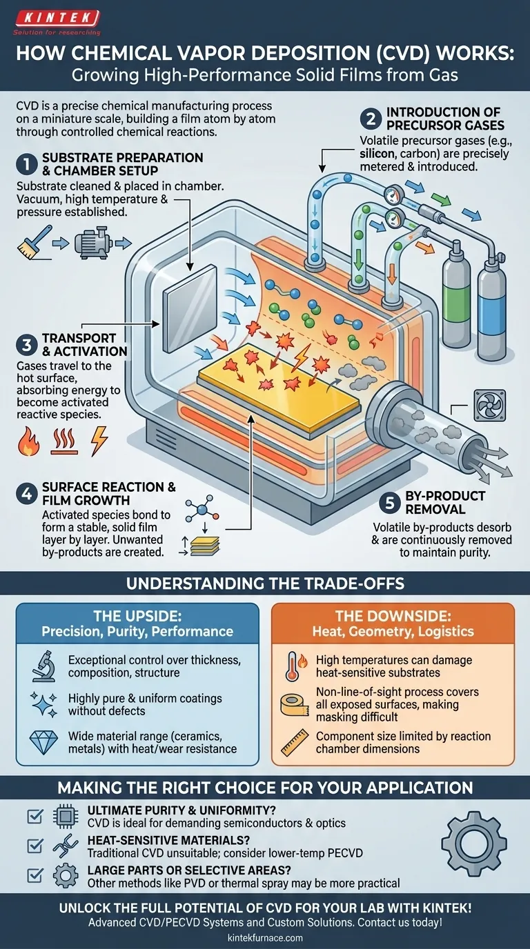
The Anatomy of a CVD Process
To truly grasp how CVD works, it's best to break it down into a sequence of controlled events. Each step is critical for achieving a high-quality, functional film.
Step 1: Substrate Preparation and Chamber Setup
Before any reaction begins, the substrate—the part to be coated—is cleaned and placed inside a sealed reaction chamber.
The chamber environment is then established. This often involves creating a vacuum to remove contaminants and then setting a specific high temperature and pressure, which are required to drive the chemical reactions.
Step 2: Introduction of Precursor Gases
Precursor gases are the "building blocks" of the film. These are volatile compounds that contain the elements needed for the final coating (e.g., silicon, carbon, titanium).
These gases are precisely metered and introduced into the chamber, flowing towards the heated substrate. The choice of precursors is dictated by the desired film material and its properties.
Step 3: Transport and Activation
The precursor gases travel through the chamber via convection and diffusion until they approach the substrate.
As the gases near the hot surface, they cross a "boundary layer" and absorb energy. This energy, typically thermal, activates the precursors, breaking them down into more reactive chemical species. In some advanced CVD methods, a plasma is used instead of high heat for this activation step.
Step 4: Surface Reaction and Film Growth
This is the heart of the CVD process. Activated chemical species adsorb onto the substrate's surface.
Once on the surface, they undergo chemical reactions, bonding with the substrate and with each other to form a stable, solid film. The film grows layer by layer, resulting in a highly uniform and dense coating.
Step 5: By-product Removal
The chemical reactions that form the film also create unwanted volatile by-products.
These gaseous by-products desorb from the surface and are carried away by the gas flow, exiting the chamber through an exhaust system. This constant removal is crucial for maintaining the purity of the film as it grows.
Understanding the Trade-offs
CVD is an exceptionally powerful technique, but its advantages come with specific operational constraints. Understanding this balance is key to deciding if it's the right solution for your problem.
The Upside: Precision, Purity, and Performance
The primary benefit of CVD is the exceptional control it offers. You can precisely manage film thickness, composition, and crystal structure, leading to highly pure and uniform coatings without defects.
This versatility allows for the deposition of a wide range of materials, including hard ceramics, diamond-like carbon, and high-purity metals, making the resulting components highly resistant to heat and wear.
The Downside: Heat, Geometry, and Logistics
The high temperatures required for traditional CVD can damage heat-sensitive substrates, limiting the materials you can coat.
Furthermore, the process is non-line-of-sight, meaning it coats every exposed surface of the part. This makes it difficult to mask specific areas. The physical size of the components is also strictly limited by the dimensions of the reaction chamber.
Making the Right Choice for Your Application
Use these guidelines to determine if CVD aligns with your project goals.
- If your primary focus is ultimate purity and uniformity: CVD is an ideal choice for demanding applications like semiconductor fabrication or optical coatings where material perfection is paramount.
- If your primary focus is coating heat-sensitive materials (like polymers or certain alloys): Traditional high-temperature CVD is likely unsuitable; you must investigate lower-temperature variants like Plasma-Enhanced CVD (PECVD).
- If your primary focus is coating very large parts or selective surface areas: The constraints of chamber size and the difficulty of masking may make other methods, like Physical Vapor Deposition (PVD) or thermal spray, a more practical fit.
Understanding this process—from precursor chemistry to its operational trade-offs—is the key to leveraging its power effectively.
Summary Table:
| CVD Process Step | Key Actions | Purpose |
|---|---|---|
| Substrate Preparation | Clean and place substrate in chamber | Ensure a contaminant-free surface for coating |
| Gas Introduction | Meter and flow precursor gases into chamber | Provide building blocks for the film material |
| Transport and Activation | Heat gases to create reactive species | Enable chemical reactions on the substrate surface |
| Surface Reaction | Adsorb and bond species to form solid film | Grow uniform, dense coating layer by layer |
| By-product Removal | Exhaust volatile by-products from chamber | Maintain film purity and continuous growth |
Unlock the full potential of CVD for your lab with KINTEK! Leveraging exceptional R&D and in-house manufacturing, we provide advanced high-temperature furnace solutions like CVD/PECVD Systems, Muffle, Tube, Rotary Furnaces, and Vacuum & Atmosphere Furnaces. Our strong deep customization capability ensures precise alignment with your unique experimental needs, delivering superior purity, uniformity, and performance for applications in semiconductors, optics, and beyond. Contact us today to discuss how our tailored solutions can elevate your research and production efficiency!
Visual Guide
Related Products
- Custom Made Versatile CVD Tube Furnace Chemical Vapor Deposition CVD Equipment Machine
- Split Chamber CVD Tube Furnace with Vacuum Station CVD Machine
- Multi Heating Zones CVD Tube Furnace Machine for Chemical Vapor Deposition Equipment
- Slide PECVD Tube Furnace with Liquid Gasifier PECVD Machine
- Inclined Rotary Plasma Enhanced Chemical Deposition PECVD Tube Furnace Machine
People Also Ask
- How might AI and machine learning enhance CVD tube furnace processes? Boost Quality, Speed, and Safety
- What are the practical applications of gate media prepared by CVD tube furnaces? Unlock Advanced Electronics and More
- What are the key features of CVD tube furnaces for 2D material processing? Unlock Precision Synthesis for Superior Materials
- Which industries and research fields benefit from CVD tube furnace sintering systems for 2D materials? Unlock Next-Gen Tech Innovations
- How does CVD tube furnace sintering enhance graphene growth? Achieve Superior Crystallinity and High Electron Mobility


