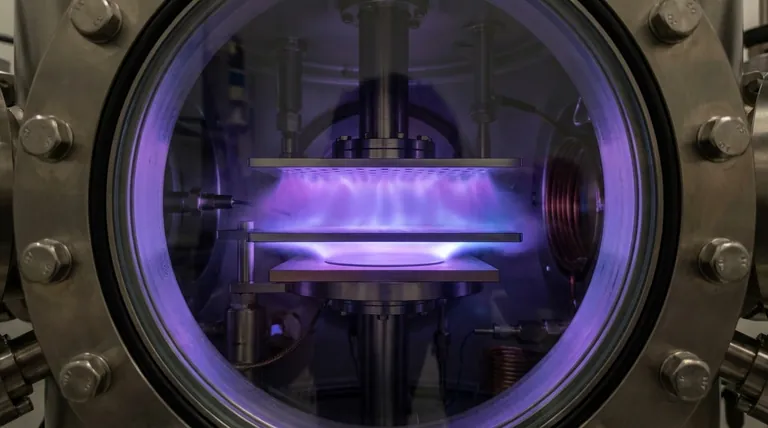
In a Plasma-Enhanced Chemical Vapor Deposition (PECVD) system, plasma is generated by applying a strong electric field to a low-pressure gas within a vacuum chamber. This field, created by applying a voltage between two electrodes, energizes the gas, stripping electrons from atoms and molecules. This process, known as ionization, creates a reactive mixture of ions, electrons, radicals, and neutral species that we call plasma.
The core purpose of generating plasma in PECVD is not just to ionize gas, but to create a highly energetic, reactive environment at a low temperature. This plasma acts as the catalyst, providing the energy to drive chemical reactions for thin-film deposition without requiring destructive high heat.
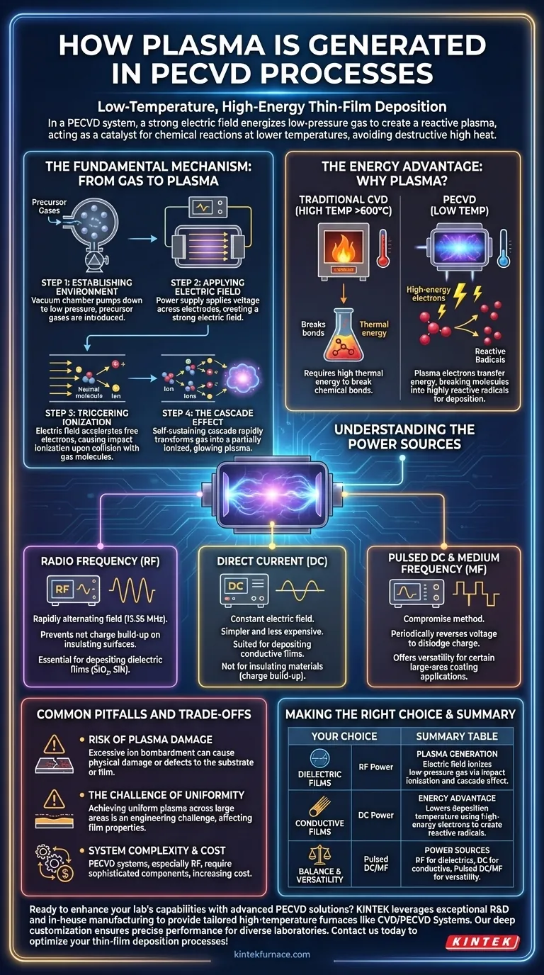
The Fundamental Mechanism: From Gas to Plasma
Understanding how a simple gas transforms into a reactive plasma is key to mastering the PECVD process. The transformation relies on a controlled chain reaction initiated by an electric field.
Step 1: Establishing the Environment
Before plasma generation, the process chamber is pumped down to a low pressure (a near-vacuum). Then, specific precursor gases are introduced. These are the gases that contain the chemical elements intended for the final thin film.
Step 2: Applying the Electric Field
A power supply applies a voltage across two electrodes inside the chamber. This creates a strong electric field in the space between them, where the precursor gases reside.
Step 3: Triggering Ionization
A few free electrons are always naturally present in the gas. The electric field accelerates these electrons to very high speeds and energies. When one of these high-energy electrons collides with a gas molecule, it can knock another electron loose.
This creates a positive ion (the original molecule minus an electron) and a new free electron. This process is called impact ionization.
Step 4: The Cascade Effect
The newly freed electron is also accelerated by the electric field, leading to more collisions and more ionization. This creates a self-sustaining cascade effect, rapidly transforming the neutral gas into a partially ionized, glowing plasma. The glow itself is a result of excited particles releasing energy as light.
Why Use Plasma? The Energy Advantage
The primary reason for using plasma is to lower the temperature required for deposition. In conventional Chemical Vapor Deposition (CVD), high temperatures (often >600°C) are needed to provide the thermal energy to break chemical bonds in the precursor gases.
Energy Transfer via Electrons
In PECVD, the energy to drive these reactions comes from the plasma itself. The high-energy electrons transfer their energy to the gas molecules through collisions. This breaks the molecules into highly reactive fragments called radicals.
Low-Temperature Deposition
These radicals are far more chemically reactive than the original precursor gas molecules. They readily adsorb onto the substrate surface and form the desired thin film, all without needing high substrate temperatures. This allows for deposition on temperature-sensitive materials like plastics or complex microelectronic devices.
Understanding the Power Sources
The choice of power supply is critical as it directly influences the plasma's characteristics and, consequently, the properties of the deposited film.
Radio Frequency (RF)
RF power (typically at 13.56 MHz) is the most common method. The rapidly alternating electric field is effective at energizing electrons. Critically, because the field is always changing, it prevents a net charge from building up on insulating surfaces. This makes RF essential for depositing dielectric films like silicon dioxide (SiO₂) and silicon nitride (SiN).
Direct Current (DC)
DC power uses a constant electric field. It is simpler and often less expensive than RF. However, it can only be used to deposit conductive films. If used with an insulating material, charge would build up on the surface, creating an opposing electric field that quickly extinguishes the plasma.
Pulsed DC and Medium Frequency (MF)
Pulsed DC and MF power supplies offer a compromise. By periodically pulsing or reversing the voltage, they can dislodge the charge build-up on semi-insulating surfaces. This provides more versatility than standard DC while being less complex than high-frequency RF systems, making it a good choice for certain large-area coating applications.
Common Pitfalls and Trade-offs
While powerful, plasma is not a perfect solution. The energetic nature of the process introduces complexities that must be managed.
Risk of Plasma Damage
The positive ions created in the plasma are accelerated by the electric field and bombard the substrate surface. This bombardment can be beneficial, increasing film density, but excessive energy can cause physical damage to the substrate or the growing film, creating defects.
The Challenge of Uniformity
Achieving a perfectly uniform plasma across a large substrate is a major engineering challenge. Any non-uniformity in plasma density or energy will directly translate into variations in film thickness and material properties, which is unacceptable for high-precision applications.
System Complexity and Cost
PECVD systems, particularly those using RF power, are more complex than their thermal CVD counterparts. They require sophisticated power supplies, impedance matching networks to efficiently transfer power to the plasma, and advanced chamber designs, all of which increase cost.
Making the Right Choice for Your Goal
Your choice of plasma generation method is determined by the material you are depositing and your process requirements.
- If your primary focus is depositing high-quality dielectric (insulating) films: RF power is the industry standard, as it effectively prevents charge build-up and provides a stable, controllable plasma.
- If your primary focus is depositing conductive films at a lower cost: A DC power supply is a simpler and more economical solution that is perfectly suited for this task.
- If your primary focus is balancing performance and cost for large-area coatings: Pulsed DC or MF systems can offer a practical middle ground, providing better process control than DC without the full complexity of an RF system.
Ultimately, understanding plasma generation is about understanding how to precisely control energy to build materials atom by atom.
Summary Table:
| Aspect | Key Details |
|---|---|
| Plasma Generation | Electric field ionizes low-pressure gas via impact ionization and cascade effect. |
| Energy Advantage | Lowers deposition temperature using high-energy electrons to create reactive radicals. |
| Power Sources | RF for dielectrics, DC for conductive films, Pulsed DC/MF for versatility. |
| Common Pitfalls | Risk of plasma damage, uniformity challenges, and higher system complexity. |
Ready to enhance your lab's capabilities with advanced PECVD solutions? KINTEK leverages exceptional R&D and in-house manufacturing to provide high-temperature furnaces like CVD/PECVD Systems, tailored to your unique experimental needs. Our deep customization ensures precise performance for diverse laboratories. Contact us today to discuss how we can optimize your thin-film deposition processes!
Visual Guide
Related Products
- RF PECVD System Radio Frequency Plasma Enhanced Chemical Vapor Deposition
- Slide PECVD Tube Furnace with Liquid Gasifier PECVD Machine
- Inclined Rotary Plasma Enhanced Chemical Deposition PECVD Tube Furnace Machine
- Inclined Rotary Plasma Enhanced Chemical Deposition PECVD Tube Furnace Machine
- Cylindrical Resonator MPCVD Machine System for Lab Diamond Growth
People Also Ask
- What is RF in PECVD? A Critical Control for Plasma Deposition
- How is silicon dioxide deposited from tetraethylorthosilicate (TEOS) in PECVD? Achieve Low-Temperature, High-Quality SiO2 Films
- What is PECVD specification? A Guide to Choosing the Right System for Your Lab
- What are some promising applications of PECVD-prepared 2D materials? Unlock Advanced Sensing and Optoelectronics
- What is the role of RF power in PECVD and how does the RF-PECVD process work? Master Thin Film Deposition Control


