At its core, Plasma-Enhanced Chemical Vapor Deposition (PECVD) achieves its remarkable versatility by separating the energy source for chemical reactions from the substrate's temperature. By using an electromagnetic field to create a plasma, PECVD generates highly reactive chemical species at low temperatures, giving operators precise, independent control over the parameters that define a thin film's final properties.
The fundamental advantage of PECVD is its ability to decouple the reaction energy from thermal energy. This allows for the deposition of high-quality, dense films at temperatures low enough to protect sensitive underlying structures, while providing multiple independent "levers" to fine-tune the film's characteristics.
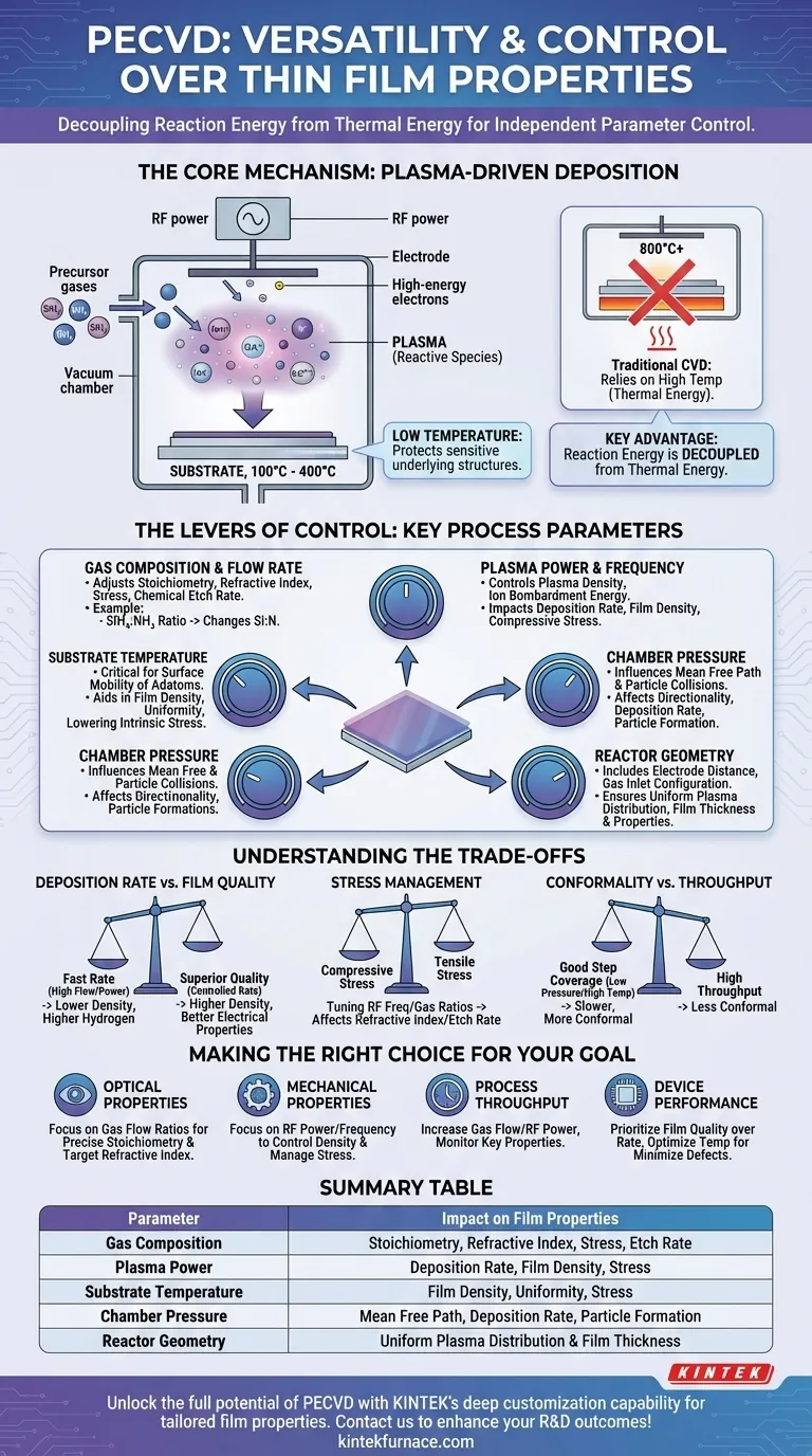
The Core Mechanism: Plasma-Driven Deposition
To understand PECVD's control, you must first understand its fundamental departure from traditional Chemical Vapor Deposition (CVD), which relies solely on high temperatures to drive reactions.
Creating Reactive Species at Low Temperatures
In a PECVD system, precursor gases like silane (SiH₄) are introduced into a vacuum chamber. An applied RF (radio frequency) electrical field energizes free electrons, which then collide with the neutral gas molecules.
These high-energy collisions break the gas molecules apart into a mix of ions, radicals, and other excited species, collectively known as plasma. These radical species are highly reactive and readily bond to the substrate surface to form a film.
Decoupling Energy from Temperature
The energy for breaking down the precursor gases comes from the plasma, not from heating the substrate. This is the single most important concept.
Because the substrate does not need to be heated to 800°C or higher (as in some thermal CVD processes), PECVD can deposit films at a much lower temperature, typically between 100°C and 400°C. This protects pre-existing device structures, such as aluminum interconnects on a microchip, from thermal damage.
The Levers of Control: Key Process Parameters
The versatility of PECVD comes from the ability to independently adjust several process parameters, each influencing the plasma environment and, consequently, the final film.
Gas Composition and Flow Rate
The specific gases introduced into the chamber and their relative flow rates directly determine the film's stoichiometry, or chemical composition.
For example, when depositing silicon nitride (SiNₓ), adjusting the ratio of silane (SiH₄) to ammonia (NH₃) will change the silicon-to-nitrogen ratio in the final film. This directly impacts the film's refractive index, stress, and chemical etch rate.
Plasma Power and Frequency
The RF power applied to the electrodes controls the plasma density and the energy of ion bombardment.
Higher power generally increases the dissociation of precursor gases, leading to a faster deposition rate. However, it also increases ion bombardment on the substrate, which can increase film density and compressive stress but may also cause damage if not controlled.
Substrate Temperature
While PECVD is a "low-temperature" process, the substrate temperature is still a critical control knob.
Modest heating provides surface mobility to the arriving atoms (adatoms), allowing them to find lower-energy sites. This helps create a denser, more uniform film with lower intrinsic stress.
Chamber Pressure
The operating pressure inside the chamber influences the mean free path of particles—the average distance a particle travels before colliding with another.
Lower pressure results in fewer gas-phase collisions and more directional deposition, while higher pressure can increase deposition rate and the potential for unwanted particle formation.
Reactor Geometry
The physical design of the reactor, including the distance between electrodes and the gas inlet configuration, directly affects the uniformity of the plasma.
A well-designed reactor ensures the plasma is evenly distributed across the substrate, resulting in a film with uniform thickness and properties from the center to the edge.
Understanding the Trade-offs
Achieving a specific film property often involves balancing competing factors. True process control requires understanding these trade-offs.
Deposition Rate vs. Film Quality
Often, the fastest deposition conditions do not produce the highest quality film. Increasing gas flow and RF power to maximize throughput can lead to lower film density, higher hydrogen content, and poorer electrical properties. A slower, more controlled deposition usually yields a superior film.
Stress Management
Nearly all deposited films have some level of intrinsic stress (either compressive or tensile), which can cause wafers to bow or films to crack. While parameters like RF frequency and gas ratios can be used to tune stress toward a neutral state, these adjustments will almost certainly affect other key properties like the refractive index or etch rate.
Conformality and Step Coverage
Covering complex, three-dimensional topography is a significant challenge. While PECVD can be optimized for better conformality, it is generally less conformal than processes like Atomic Layer Deposition (ALD). Achieving good step coverage often requires lower pressures and higher temperatures to promote surface diffusion, which may conflict with other process goals like high throughput.
Making the Right Choice for Your Goal
Your specific application will determine which parameters are most critical to control.
- If your primary focus is optical properties (e.g., anti-reflection coatings): Concentrate on precisely controlling the gas flow ratios to lock in the stoichiometry and achieve the target refractive index.
- If your primary focus is mechanical properties (e.g., hard masks or passivation layers): Focus on tuning RF power and frequency to control film density and manage intrinsic stress.
- If your primary focus is process throughput: Carefully increase gas flow rates and RF power, while continuously monitoring key film properties to ensure they remain within your acceptable process window.
- If your primary focus is device performance (e.g., gate dielectrics): Prioritize film quality over rate, using optimized temperature and a slower deposition to minimize defects and ensure excellent electrical characteristics.
By understanding these fundamental levers and their interactions, you can move from simply using a recipe to truly engineering a material for its intended function.
Summary Table:
| Parameter | Impact on Film Properties |
|---|---|
| Gas Composition | Determines stoichiometry, refractive index, stress, and etch rate |
| Plasma Power | Influences deposition rate, film density, and stress |
| Substrate Temperature | Affects film density, uniformity, and stress |
| Chamber Pressure | Controls mean free path, deposition rate, and particle formation |
| Reactor Geometry | Ensures uniform plasma distribution and film thickness |
Unlock the full potential of PECVD for your laboratory! Leveraging exceptional R&D and in-house manufacturing, KINTEK provides diverse labs with advanced high-temperature furnace solutions, including CVD/PECVD Systems. Our strong deep customization capability ensures we precisely meet your unique experimental requirements for tailored film properties. Contact us today to discuss how our expertise can enhance your research and development outcomes!
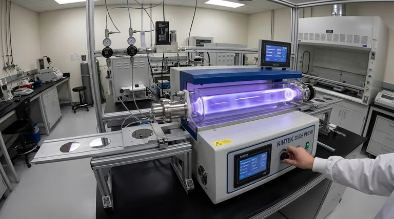
Visual Guide
Related Products
- Slide PECVD Tube Furnace with Liquid Gasifier PECVD Machine
- RF PECVD System Radio Frequency Plasma Enhanced Chemical Vapor Deposition
- Inclined Rotary Plasma Enhanced Chemical Deposition PECVD Tube Furnace Machine
- Inclined Rotary Plasma Enhanced Chemical Deposition PECVD Tube Furnace Machine
- Multi Heating Zones CVD Tube Furnace Machine for Chemical Vapor Deposition Equipment
People Also Ask
- How does PECVD equipment contribute to TOPCon bottom cells? Mastering Hydrogenation for Maximum Solar Efficiency
- How does a hydrogen reduction environment in an industrial tube furnace facilitate gold-copper alloy microspheres?
- What is plasma in the context of PECVD? Unlock Low-Temperature Thin Film Deposition
- What are the disadvantages of tube furnace cracking when processing heavy raw materials? Avoid Costly Downtime and Inefficiency
- What are the advantages of using a tube furnace CVD system for Cu(111)/graphene? Superior Scalability and Quality


