The relationship between thermal processing, polarization, and performance in BaTiO3 ceramics is one of cause and effect. Controlled high-temperature sintering first establishes the fundamental microstructure—grain size, density, and porosity—which dictates the types and concentrations of defects present. A subsequent polarization treatment then actively annihilates many of these defects, particularly at grain boundaries, and creates internal electric fields that suppress charge migration, resulting in a dramatically lower dielectric loss factor.
The core takeaway is that sintering and polarization work in sequence, not isolation. Precise thermal control builds a "high-quality canvas" by minimizing intrinsic porosity; high-voltage polarization then "finishes the work" by passivating the remaining defective regions, primarily at grain boundaries. The final dielectric loss is a direct report card on how well both steps were executed.
The Foundational Role of Controlled Thermal Processing
The initial sintering process is not just about making a ceramic dense. It is the foundational step that defines the entire defect landscape of the material.
How Sintering Temperature Governs the Defect Structure
The peak temperature and soak time during sintering directly control the population of extrinsic defects. These are the imperfections—porosity, microcracks, and grain boundary anomalies—that are devourers of electromagnetic energy.
Firing at sufficiently high temperatures, for example, achieving 78%–83.5% of theoretical density, minimizes these structural flaws. Think of it as drawing a picture. A low-temperature, incomplete sinter is like a sketch with many broken lines and gaps. A high-temperature, well-soaked sinter creates a continuous, dense network, providing the ideal foundation for electrical stability. Conversely, a short soak time can leave behind a "skeleton" of interconnected pores, a major source of dielectric loss.
Grain Size, Domain Walls, and Intrinsic Loss
Thermal processing also dictates grain morphology, which has a complex relationship with dielectric loss. Increasing the sintering temperature from 1240°C to 1370°C causes discontinuous grain growth, shifting average grain sizes from 10–20 µm up to 20–50 µm.
This matters because larger grains contain wider domain structures. The domain walls themselves can contribute to intrinsic loss. Therefore, a furnace capable of precise, uniform thermal control is not just a heating device; it's a tool for engineering specific domain configurations to balance other properties like permittivity with loss.
The Crucial Influence of Heating Rate
The journey to the peak temperature is as critical as the destination. The thermal ramp rate directly affects densification and grain boundary development.
A poorly controlled ramp can trap gases, creating residual porosity, or cause uneven grain growth. A precisely controlled, programmable furnace profile ensures uniform densification and complete organic burnout, systematically eliminating the micro-voids that would otherwise dissipate signal energy. The goal is a homogeneous, defect-minimized body before polarization even begins.
How Polarization Annihilates Defects and Suppresses Loss
Even the best-sintered ceramic is imperfect. The polarization step is an active process that hunts down and neutralizes the remaining problematic regions.
Passivating Grain Boundaries and Pores
When a high-voltage DC field is applied at an elevated temperature, it forces the ceramic's ferroelectric domains to align. More importantly, it drives charge carriers toward grain boundaries and internal pores.
These interfaces are high-energy, defective regions where charge carriers typically become trapped and then hop around under an AC field, a primary mechanism for dielectric loss. The polarization process annihilates these defects by filling traps and reorganizing the space charge. This creates a stable, passivated interface that is far less electrically active, directly attacking the root cause of loss.
Building an Internal Anti-Loss Field
The reoriented ferroelectric domains and stabilized space charge layers generate a persistent internal electric field. This internal field acts as a barrier, inhibiting the hopping of charge carriers between defects.
Without polarization, these carriers move freely under an applied AC signal, dissipating energy as heat (high tgδ). The internal field clamps down on this movement, significantly reducing the dielectric loss factor. It's not about creating a perfect crystal; it's about building an internal defense network that suppresses the activity of the imperfections that remain.
Understanding the Synergy and Its Limits
The final performance is a product of the entire process chain. A brilliant polarization step cannot fix a fundamentally flawed microstructure, and a perfect sinter can still exhibit high losses without poling.
Why Initial Microstructure Dictates Poling Success
Poling a poorly sintered ceramic with high porosity and microcracks is ineffective and dangerous. The high-voltage field will concentrate in these voids, likely causing dielectric breakdown and catastrophic failure.
The initial thermal processing must therefore deliver a dense ceramic with minimal critical flaws. High-precision laboratory furnaces are essential here, providing the uniform thermal distribution that prevents localized stresses and ensures every part of the ceramic body is equally ready for the high-voltage treatment. The sinter creates the foundation; polarization only optimizes it.
Common Pitfalls to Avoid
Misunderstanding the process sequence leads to predictable failures. One common mistake is treating the sintering furnace as a simple "oven" and not as a primary microstructural engineering tool. Using a furnace with poor temperature uniformity or a non-programmable controller can create a ceramic with a wide variation in grain size and density in a single batch.
Another pitfall is applying the polarization field at room temperature or with an insufficient voltage. This fails to mobilize the space charge needed to passivate grain boundaries. The result is a ceramic with visually aligned domains but no internal field to suppress charge hopping, leading to a higher than expected dielectric loss factor that cannot be corrected.
Making the Right Choice for Your Application
Your specific goal determines whether you should focus more on optimizing the sintering profile or the polarization parameters.
- If your primary focus is minimizing dielectric loss for high-frequency applications: Direct your efforts at the sintering stage to minimize extrinsic defects. Use a furnace with precise multi-segment control for slow, uniform densification to virtually eliminate porosity, as this is the dominant loss mechanism.
- If your primary focus is stabilizing and reducing loss in a sensor or actuator: The polarization process is your most critical step. Ensure your sintered ceramic is dense enough to survive poling, then focus on optimizing the temperature and field strength of the polarization treatment to build a robust internal field that suppresses charge carrier hopping.
- If your primary focus is achieving a specific balance of high permittivity and low loss: You must tightly integrate both steps. Use the furnace's thermal profile to engineer a target grain size that gives desired permittivity, and then use polarization to passivate the grain boundaries of that specific microstructure, suppressing the loss without sacrificing the density or domain structure.
A low dielectric loss factor is not a property you simply measure; it is an achievement that is carefully engineered through a sequence of thermal and electrical control.
Summary Table:
| Processing Stage | Primary Defect & Microstructural Mechanism | Impact on Dielectric Loss |
|---|---|---|
| Controlled Sintering | Minimizes porosity and microcracks; governs grain size and domain wall density. | Eliminates extrinsic loss pathways; sets the dense foundation to prevent dielectric breakdown. |
| Polarization Treatment | Passivates grain boundaries; traps space charge and reorganizes internal defect states. | Builds an internal electric field that suppresses charge carrier hopping, dramatically lowering tgδ. |
| Integrated Synergy | Combines uniform high-density sintering with optimal high-voltage field poling. | Delivers optimized permittivity alongside ultra-low dielectric loss for high-performance applications. |
Engineer Superior Dielectric Materials with KINTEK High-Temperature Furnaces
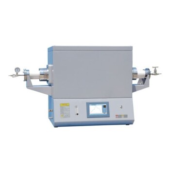
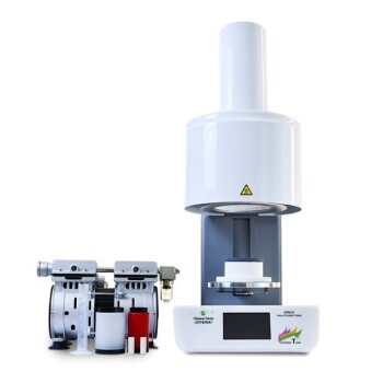
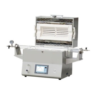
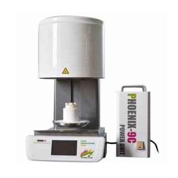
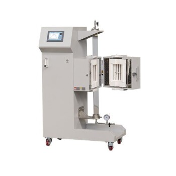
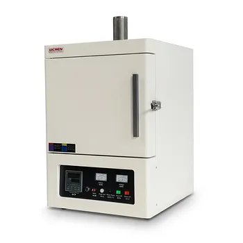
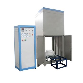
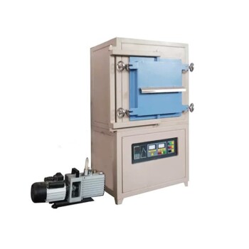
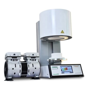
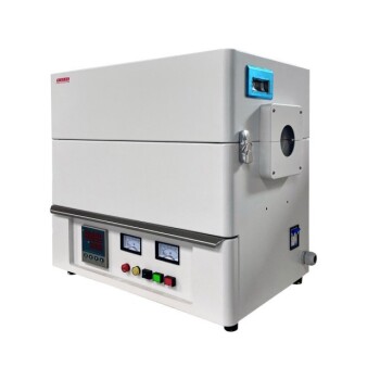
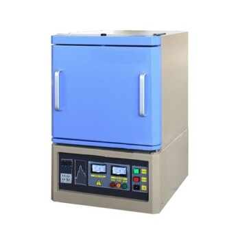
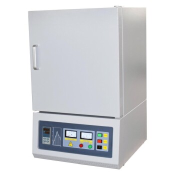
Achieving ultra-low dielectric loss and precise microstructural control in BaTiO3 ceramics requires flawless thermal execution. KINTEK specializes in advanced laboratory equipment and consumables, offering a comprehensive lineup of customizable high-temperature furnaces—including muffle, tube, atmosphere, vacuum, CVD, rotary, and induction melting furnaces.
Our precision-engineered furnaces deliver the exact multi-segment temperature control, programmable ramp rates, and exceptional thermal uniformity necessary to eliminate porosity, optimize grain growth, and prevent defect formation prior to polarization.
Take control of your ceramic sintering profiles today—Contact KINTEK experts now to tailor the perfect furnace solution for your research and production needs!
Related Products
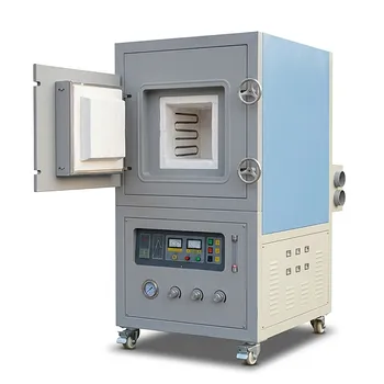
- High Temperature Muffle Oven Furnace for Laboratory Debinding and Pre Sintering
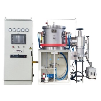
- 2200 ℃ Tungsten Vacuum Heat Treat and Sintering Furnace
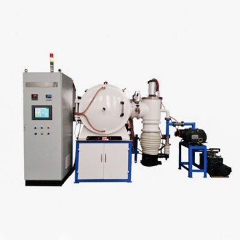
- 2200 ℃ Graphite Vacuum Heat Treat Furnace
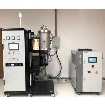
- Vacuum Heat Treat Sintering Furnace Molybdenum Wire Vacuum Sintering Furnace
- 1700℃ High Temperature Laboratory Tube Furnace with Alumina Tube
People Also Ask
- What thermal phenomena occur during polymer binder burnout in ceramic green bodies? Lab Furnace Guide
- What role does a high-temperature muffle furnace play in STFO synthesis? Achieve Pure Perovskite Results
- Why is controlled heat treatment in a muffle furnace necessary for calcined clay? Achieve Optimal Pozzolanic Activity
- How does a high-temperature muffle furnace facilitate the formation of LaNbxAl1−xO3+δ perovskite structures? Key Roles
- What role does a high-temperature muffle furnace play in the formation of biochar catalysts? Master Catalyst Synthesis