At their core, chemical vapor deposition (CVD) and physical vapor deposition (PVD) are fundamentally different in their mechanics. PVD is a physical process that involves vaporizing a solid material and having it condense onto a substrate, much like spray painting. In contrast, CVD is a chemical process where gas precursors are introduced into a chamber and react on the substrate's surface to form the desired film.
The choice between CVD and PVD is not about which is "better," but which process aligns with your application's geometry and material constraints. PVD physically transports material in a line-of-sight, while CVD chemically builds a film on all exposed surfaces simultaneously.
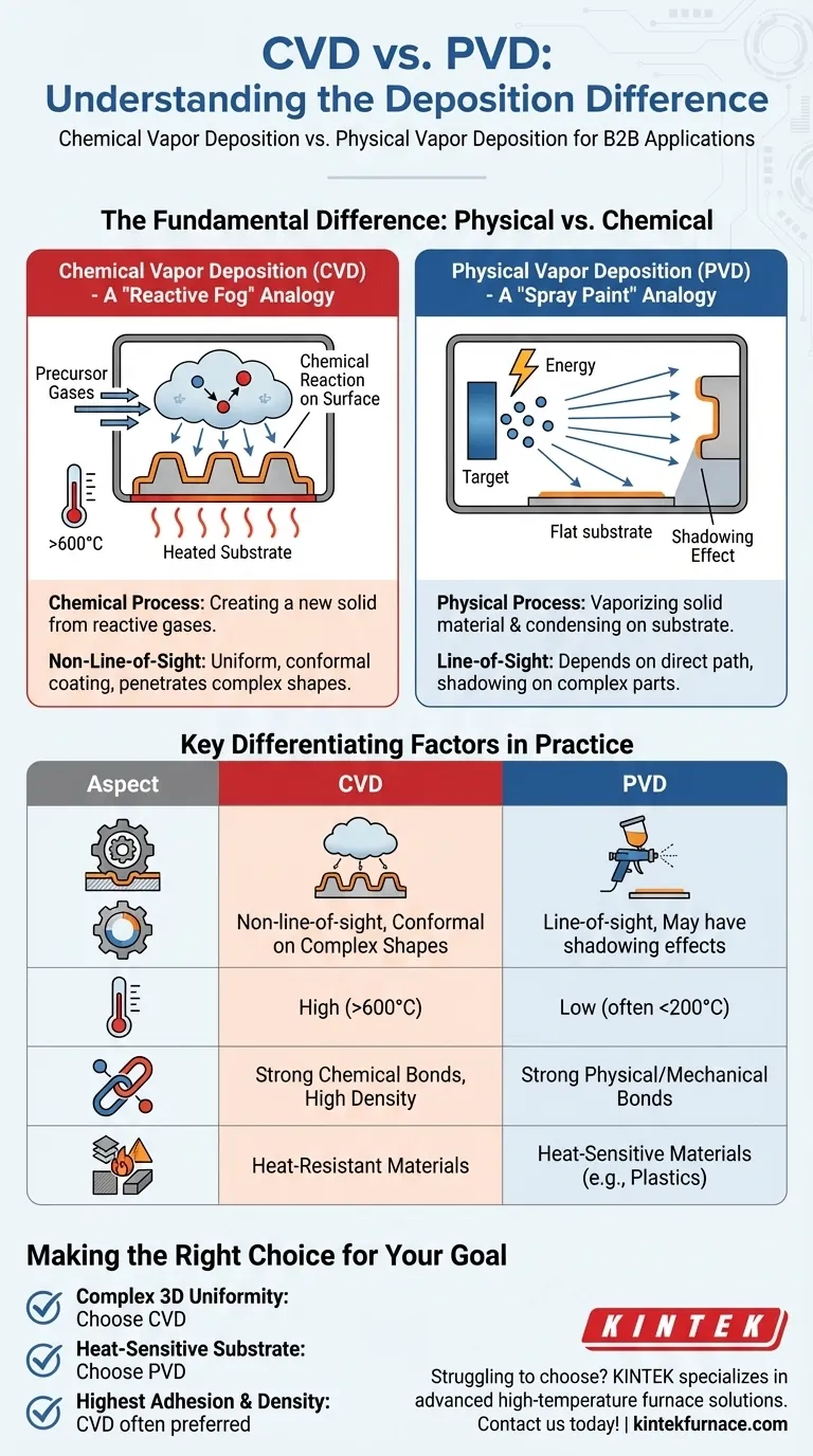
The Fundamental Difference: Physical vs. Chemical
The names themselves reveal the primary distinction. One process relies on physics (state changes from solid to vapor to solid), while the other relies on chemistry (creating a new solid from reactive gases).
Physical Vapor Deposition (PVD): A "Spray Paint" Analogy
In PVD, a solid source material, known as a target, is bombarded with energy inside a vacuum chamber. This energy (often from ions in a process like sputtering) ejects atoms from the target, creating a vapor.
These vaporized atoms travel in a straight line and condense on any surface they hit, including your part (the substrate). This is why PVD is considered a line-of-sight process.
Chemical Vapor Deposition (CVD): A "Reactive Fog" Analogy
CVD does not start with a solid block of the coating material. Instead, it uses volatile precursor gases containing the required chemical elements.
These gases are introduced into a vacuum chamber containing the heated substrate. The heat provides the energy needed to trigger a chemical reaction on the substrate's surface, where the precursors decompose and form a solid, stable film atom by atom. The leftover gaseous byproducts are then pumped out.
Key Differentiating Factors in Practice
The mechanical difference between PVD and CVD creates significant practical consequences for uniformity, temperature, and film quality.
Coating Uniformity and Geometry
This is the most critical distinction for many applications. Because CVD uses a gas that fills the entire chamber, it is a non-line-of-sight process.
It excels at creating highly conformal and uniform coatings over complex shapes, inside tubes, and on intricate 3D surfaces. The reactive gas can penetrate any area the substrate is exposed to.
PVD, being line-of-sight, struggles with this. It creates a "shadowing" effect, where areas not directly facing the source receive little to no coating.
Process Temperature
CVD processes typically require high temperatures (often >600°C) to provide the activation energy needed to drive the chemical reactions on the substrate surface.
PVD processes can often be performed at much lower temperatures (sometimes below 200°C), making them suitable for coating materials that cannot withstand high heat, such as plastics or certain metal alloys.
Film Properties and Adhesion
Because CVD films are grown through chemical reactions, they form strong chemical bonds with the substrate material. This can result in exceptional adhesion and a very dense, high-purity film.
PVD films adhere through physical and mechanical bonding, which is typically very strong but can be more sensitive to surface preparation and deposition parameters.
Understanding the Trade-offs
Neither method is universally superior. The optimal choice requires understanding their inherent limitations.
The Limitations of CVD
The primary drawback of CVD is its high process temperature, which restricts the types of substrates that can be coated without being damaged or warped.
Additionally, the precursor gases used in CVD can be highly toxic, flammable, or corrosive, necessitating complex and expensive safety and handling systems.
The Limitations of PVD
The most significant limitation of PVD is its line-of-sight nature. This makes it unsuitable for uniformly coating complex parts without sophisticated and often costly part-rotation mechanisms.
Achieving perfect film stoichiometry (the exact chemical ratio of elements) can also be more challenging in some PVD processes compared to the precise control offered by CVD's gas-phase chemistry.
Making the Right Choice for Your Goal
Your decision should be guided by the non-negotiable requirements of your component and its application.
- If your primary focus is coating a complex 3D part uniformly: CVD is the clear choice due to its non-line-of-sight nature and ability to create conformal films.
- If your primary focus is coating a heat-sensitive substrate: PVD is the better starting point, as its lower operating temperatures prevent damage to materials like polymers or aluminum alloys.
- If your primary focus is achieving the highest possible adhesion and film density: CVD often has an advantage due to the chemical bonds formed, though high-quality PVD can also produce excellent results.
By understanding the core mechanism—physical transport versus chemical reaction—you can confidently select the right deposition strategy for your specific engineering challenge.
Summary Table:
| Aspect | Chemical Vapor Deposition (CVD) | Physical Vapor Deposition (PVD) |
|---|---|---|
| Process Type | Chemical reaction on substrate | Physical vaporization and condensation |
| Coating Uniformity | Non-line-of-sight, conformal on complex shapes | Line-of-sight, may have shadowing effects |
| Process Temperature | High (>600°C) | Low (often <200°C) |
| Film Adhesion | Strong chemical bonds, high density | Strong physical/mechanical bonds |
| Suitable Substrates | Heat-resistant materials | Heat-sensitive materials (e.g., plastics) |
Struggling to choose between CVD and PVD for your lab's needs? At KINTEK, we specialize in advanced high-temperature furnace solutions, including CVD/PECVD Systems, tailored to diverse laboratory requirements. Leveraging our exceptional R&D and in-house manufacturing, we offer deep customization to precisely meet your unique experimental challenges—ensuring optimal performance, efficiency, and reliability. Don't let deposition dilemmas hold you back; contact us today to discuss how our expertise can elevate your research and development!
Visual Guide
Related Products
- Custom Made Versatile CVD Tube Furnace Chemical Vapor Deposition CVD Equipment Machine
- RF PECVD System Radio Frequency Plasma Enhanced Chemical Vapor Deposition
- MPCVD Machine System Reactor Bell-jar Resonator for Lab and Diamond Growth
- 915MHz MPCVD Diamond Machine Microwave Plasma Chemical Vapor Deposition System Reactor
- Slide PECVD Tube Furnace with Liquid Gasifier PECVD Machine
People Also Ask
- What is a CVD tube furnace and what is its primary function? Discover Precision Thin-Film Deposition
- How does CVD tube furnace sintering enhance graphene growth? Achieve Superior Crystallinity and High Electron Mobility
- Why are CVD tube furnace sintering systems indispensable for 2D material research and production? Unlock Atomic-Scale Precision
- What are the key features of CVD tube furnaces for 2D material processing? Unlock Precision Synthesis for Superior Materials
- What is the working principle of a CVD tube furnace? Achieve Precise Thin Film Deposition for Your Lab


