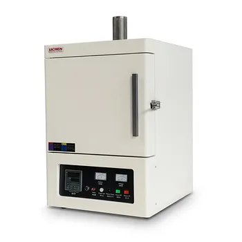
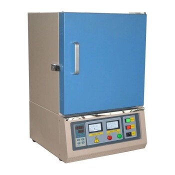
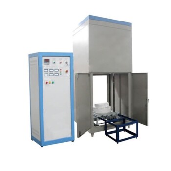
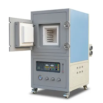
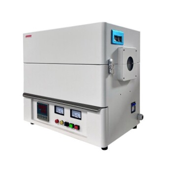
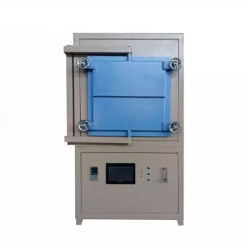
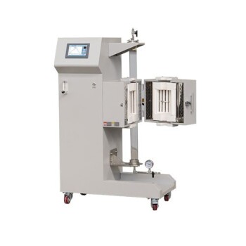
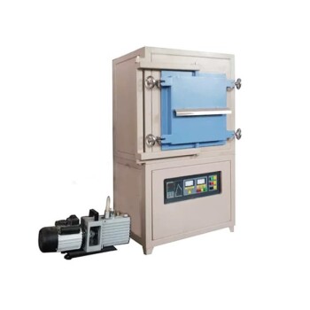
Sintering temperature is the master switch that governs grain growth and domain architecture in barium titanate.
Raising the peak temperature from 1240°C to 1370°C in a high‑temperature laboratory furnace drives grain size from 10–20 µm up to 50 µm and beyond, triggering a fundamental shift from single‑domain patterns to complex banded ferroelectric domains. The heating rate, dwell time, and pressing pressure all contribute, but the thermal profile is what ultimately dictates whether your ceramic’s microstructure will be dominated by fine, single‑domain grains or coarse, banded‑domain structures.
The sintering temperature defines the grain size, which serves as a structural threshold for domain configuration. Fine grains (typically below ~40–60 µm) yield single‑domain patterns, while coarse grains develop banded domains whose width then scales with grain size—a relationship that precise furnace control allows you to harness for specific electrical properties.
How Sintering Temperature Drives Grain Growth
The Temperature Window for BaTiO₃ Densification
In pure BaTiO₃, increasing the sintering temperature from 1180°C to 1370°C raises bulk density from about 3.2 × 10³ kg/m³ to 3.6 × 10³ kg/m³.
Higher temperatures accelerate diffusion transport mechanisms at inter‑particle necks, transforming spherical grains into interconnected ellipsoidal shapes and eliminating porosity.
At 1240°C, discontinuous grain growth produces grains of 10–20 µm.
At 1370°C, the microstructure coarsens dramatically, yielding average grain sizes of 20–50 µm and occasionally grains as large as 100 µm.
Heating Rate and Dwell Time: Fine‑Tuning the Microstructure
Thermal analysis shows that BaCO₃ decarbonization begins around 850°C regardless of ramp rate, while the solid‑state reaction between BaO and TiO₂ initiates at ~970°C.
However, when you increase the heating rate from 4°C/min to 30°C/min, the completion of that solid‑state reaction and the maximum shrinkage stage shift to higher temperatures.
Excessively fast ramps reduce the thermal exposure time required for complete solid‑state conversion and optimal densification.
A balanced ramp rate, combined with a well‑controlled dwell time at the peak temperature, ensures full reaction, uniform grain growth, and the targeted grain size distribution.
The Influence of Dopants: Restricting Grain Growth
Doping with elements such as calcium acts as a potent grain growth inhibitor during sintering at 1240–1370°C.
While pure BaTiO₃ forms coarse, banded grains, Ca‑modified compositions (e.g., (Ba,Pb,Ca)TiO₃) consistently maintain a fine‑grained microstructure averaging 1–3 µm.
This dramatic grain refinement forces the ceramic into a predominantly single‑domain structure with domain widths of only 0.1–0.3 µm and wall thicknesses of 0.05–0.15 µm.
Precise thermal profiles are critical to distribute dopants uniformly and lock in that fine‑grained, single‑domain state.
The Grain Size–Domain Structure Connection
The ~40–60 µm Threshold: Where Domain Behavior Changes
At grain sizes below approximately 40–60 µm, the ceramic typically exhibits a single‑domain pattern in each grain.
Above this critical threshold, the domain landscape transforms into banded domain structures made of 90° and 180° domain walls arranged in herringbone or square‑net patterns.
Remarkably, domain behavior then splits into two distinct regimes.
For grains up to ~60 µm, the band domain size is relatively insensitive to grain size variations. Once grains exceed 60 µm and approach 100 µm, band domain dimensions increase proportionally with grain size, and domain boundaries can extend fully across individual grains.
Banded Domain Patterns in Coarse Grains
The classic banded configuration in pure BaTiO₃ appears in grains larger than ~40 µm, with domain widths ranging from 0.5 µm to 1.2 µm.
These 90° and 180° walls create the herringbone and square‑net motifs that directly influence dielectric permittivity and losses through domain wall mobility.
Single‑Domain Regions in Fine‑Grained Ceramics
When sintering conditions—whether lower temperatures or grain‑growth inhibitors like Ca—yield grain sizes well below 40 µm, the ceramic is largely single‑domain.
In these materials, domain wall density is minimal, which can translate to lower polarization reversal contributions and reduced dielectric losses, making them attractive for stable, high‑frequency applications.
Precision Furnace Control Enables Property Optimization
Tailoring Dielectric and Ferroelectric Performance
Domain wall density, governed by grain size, is a direct lever on the dielectric constant and loss tangent.
Finely controlled thermal cycles allow you to target a specific grain size and thus a predictable domain architecture, whether you want higher dielectric permittivity from mobile banded domain walls or stable, low‑loss behavior from single‑domain grains.
Engineering the PTCR Effect Through Grain Boundary Design
For positive temperature coefficient of resistance (PTCR) thermistors, sintering between 1320°C and 1380°C is essential.
At these elevated temperatures, donor or acceptor dopants (e.g., Sb, Mn) segregate to grain boundaries, forming semiconducting grains enclosed by insulating grain boundary layers.
This microstructure creates potential barriers that, above the Curie temperature (180–190°C), produce a multi‑order‑of‑magnitude jump in resistance.
High‑temperature furnaces with excellent temperature stability guarantee reproducible electrical parameters: low Rmin, consistent Tc, and temperature coefficients of resistance up to 17.8 %/K.
Common Pitfalls and Trade‑offs in Sintering Electroceramics
- Over‑sintering and exaggerated grain growth. Holding at over‑high temperatures for too long can produce inhomogeneous grain distributions and microcracks from phase transitions, degrading both mechanical integrity and electrical uniformity.
- Rapid heating profiles. Pushing ramp rates too high shifts solid‑state reactions past the optimal temperature window, risking incomplete conversion, residual porosity, and density gradients that compromise property consistency.
- Atmosphere control neglect. BaTiO₃ is sensitive to oxygen partial pressure; poor atmosphere management during sintering can cause non‑stoichiometry, altering the defect chemistry and destabilizing the intended domain configuration.
- The single‑domain vs. banded‑domain trade‑off. Fine‑grained, single‑domain ceramics offer high electrical stability and low losses but may sacrifice maximum dielectric permittivity. Coarse‑grained, banded‑domain structures can provide a higher dielectric constant but may introduce larger losses from domain wall motion and greater sensitivity to grain size variability near the threshold region.
Making the Right Choice for Your Application
- If your primary focus is maximizing dielectric constant: Aim for larger grains that support banded domain structures by sintering at higher temperatures (~1370°C) with a controlled dwell time, ensuring grains exceed the ~40 µm threshold where band domains begin to scale with size.
- If your goal is stable, low‑loss performance (single‑domain): Sinter at lower peak temperatures (around 1240°C) or incorporate grain‑growth inhibitors like Ca to keep grain sizes well below 10 µm, forcing a single‑domain state.
- If you need a sharp, reproducible PTCR effect: Sinter at 1320–1380°C to develop the semiconducting‑grain/insulating‑barrier microstructure, and maintain tight temperature uniformity to ensure consistent dopant segregation.
- If your research demands predictable domain scaling: Target grain sizes above 60 µm, where band domain width increases in direct proportion to grain size, giving you a systematic tuning knob for domain‑wall‑related properties.
By mastering the temperature profiles of your laboratory furnace, you gain direct command over the microstructural blueprint that defines your electroceramic’s ultimate performance.
Summary Table:
| Sintering Condition | Grain Size | Domain Configuration | Key Property / Application |
|---|---|---|---|
| Low Temp (~1240°C) / Ca-Doped | Fine (1–20 µm) | Single-Domain (0.1–0.3 µm width) | Low dielectric loss, high stability for high-frequency use |
| High Temp (~1370°C) / Pure BaTiO₃ | Coarse (20–50+ µm) | Banded Domain (0.5–1.2 µm width) | High dielectric permittivity (mobile domain walls) |
| Extended Dwell (>60–100 µm) | Exaggerated (>60 µm) | Proportional Banded Domains | Direct scaling of domain width with grain size |
| 1320°C–1380°C (Doped Sb/Mn) | Engineered | Semiconducting Grain / Insulating Boundary | PTCR Thermistors (sharp multi-order resistance jump) |
Optimize Your Electroceramic Microstructures with KINTEK
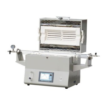
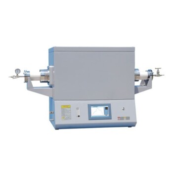
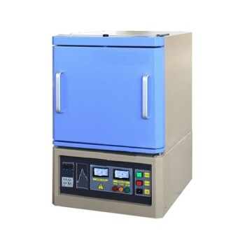
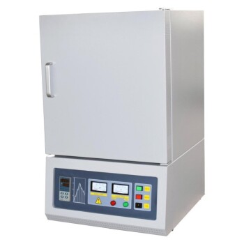
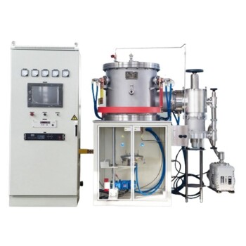
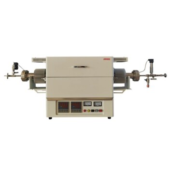
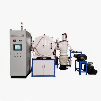
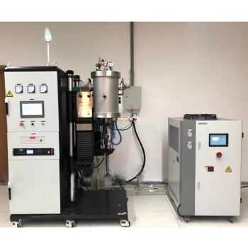
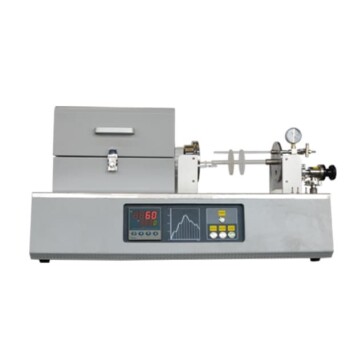
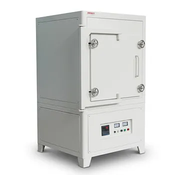
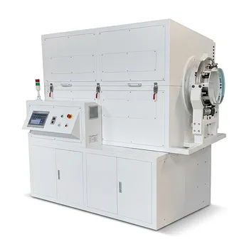
Achieving precise control over grain size, domain boundaries, and dielectric properties requires uncompromising thermal accuracy. KINTEK specializes in premium laboratory equipment and consumables, offering a comprehensive lineup of customizable high-temperature furnaces—including muffle, tube, rotary, vacuum, atmosphere, CVD, and induction melting furnaces—engineered to deliver strict temperature uniformity and atmosphere control.
Whether you are refining fine-grained $\text{BaTiO}_3$ single-domain ceramics or scaling coarse-grained PTCR thermistors, KINTEK provides tailored thermal solutions to match your exact research and production needs.
Take total command of your material performance—Contact KINTEK today to consult with our high-temperature furnace experts!
Related Products
- 1400℃ High Temperature Laboratory Tube Furnace with Alumina Tube
- 1700℃ High Temperature Laboratory Tube Furnace with Alumina Tube
- 1800℃ High Temperature Muffle Oven Furnace for Laboratory
- 1700℃ High Temperature Muffle Oven Furnace for Laboratory
- 1200℃ Muffle Oven Furnace for Laboratory
People Also Ask
- How does zone-melting in tube furnaces synthesize bismuth micro-wires? Master Single-Crystal Thermoelectric Growth
- How are high-temp tube furnaces used to measure diffusion coefficients per Fick's law? Master Precision Annealing
- How do high-temperature laboratory tube furnaces ensure environmental stability? Precision Thermal Reduction Tips
- How are high-temperature laboratory tube furnaces applied in long-term vacuum homogenization heat treatments for intermetallic samples?
- How are high-temperature tube furnaces applied in testing ceramic-supported alloy membranes? Insights