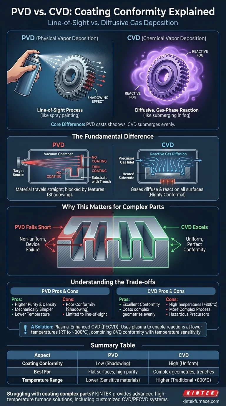
In terms of coating conformity, Chemical Vapor Deposition (CVD) is fundamentally superior to Physical Vapor Deposition (PVD). CVD processes use a gaseous precursor that uniformly coats all surfaces of a complex object, while PVD is a "line-of-sight" process that struggles to coat areas not directly exposed to the material source.
The core difference comes down to the state of the material during deposition. PVD is like spray painting, where shadows are cast behind obstacles. CVD is like submerging an object in a reactive fog, which covers every surface evenly.
The Fundamental Difference: Line-of-Sight vs. Gas Diffusion
The way each process delivers material to the substrate surface is the root cause of their difference in conformity. These mechanisms are physically distinct.
PVD: A Line-of-Sight Deposition
Physical Vapor Deposition works by physically transferring material from a source (the "target") to the substrate in a high-vacuum environment. This material travels in a straight line.
Any feature on the substrate's surface—such as a sharp corner, deep trench, or small hole—can block this path. This creates a "shadowing" effect, resulting in a much thinner coating or no coating at all on surfaces not in the direct line of sight.
CVD: A Diffusive, Gas-Phase Reaction
Chemical Vapor Deposition introduces volatile precursor gases into a reaction chamber. These gases are not "fired" at the substrate; they flow and diffuse throughout the chamber, surrounding the component on all sides.
A chemical reaction, typically activated by heat or plasma, then occurs on all exposed surfaces of the substrate. Because the gas can penetrate intricate geometries, the resulting film is highly conformal, meaning it has a uniform thickness across the entire part, including inside holes and trenches.
Why This Matters for Complex Parts
The practical implications of this difference are most significant when coating components that are not perfectly flat.
The Challenge of Coating Complex Geometries
Modern components often feature complex 3D architectures, including micro-trenches, through-holes, and undercuts. For many applications, ensuring these features are fully and evenly coated is critical for performance and reliability.
How PVD Falls Short
With its line-of-sight nature, PVD will deposit a thick layer on the top surfaces facing the source but will fail to adequately coat the sidewalls and bottoms of deep features. This non-uniformity can lead to device failure or corrosion.
Where CVD Excels
CVD's gas-phase nature ensures the reactive species reach virtually every part of the substrate's topography. This results in an exceptionally uniform film that conforms perfectly to the most complex shapes, which is why it is essential for applications like semiconductor manufacturing.
Understanding the Trade-offs
Choosing a process is not just about conformity. Each method has distinct advantages and disadvantages that make it suitable for different goals.
Purity and Simplicity of PVD
PVD processes are generally cleaner, as they involve the physical transfer of a high-purity source material. This often results in films with higher purity and density. The process is also mechanically simpler and avoids the use of hazardous precursor chemicals.
Temperature and Complexity of CVD
Traditional thermal CVD requires very high temperatures (often >800°C) to trigger the chemical reactions. This makes it unsuitable for temperature-sensitive substrates. The process is also more complex, requiring careful management of gas flows and potentially hazardous chemical precursors.
A Solution: Plasma-Enhanced CVD (PECVD)
Plasma-Enhanced CVD is a variant that uses plasma to energize the precursor gases, enabling the chemical reaction to occur at much lower temperatures (room temperature to ~300°C). PECVD combines the high-conformity advantage of CVD with the ability to coat temperature-sensitive materials.
Making the Right Choice for Your Application
The ideal coating technology is entirely dependent on your part's geometry and performance requirements.
- If your primary focus is coating complex parts with trenches, holes, or intricate geometries: CVD is the superior choice due to its excellent conformality.
- If your primary focus is depositing a very pure, dense film on a relatively flat surface: PVD offers excellent control, adhesion, and process simplicity.
- If you need to coat a temperature-sensitive material with high conformity: Investigate Plasma-Enhanced CVD (PECVD) to get the benefits of CVD at lower process temperatures.
Ultimately, your success depends on matching the physics of the deposition process to the geometric reality of your component.
Summary Table:
| Aspect | PVD (Physical Vapor Deposition) | CVD (Chemical Vapor Deposition) |
|---|---|---|
| Coating Conformity | Low (line-of-sight, shadowing effects) | High (gas diffusion, uniform coverage) |
| Best For | Flat surfaces, high purity needs | Complex geometries, trenches, holes |
| Temperature Range | Lower (suitable for sensitive materials) | Higher (traditional CVD >800°C; PECVD lower) |
Struggling with coating complex parts? KINTEK leverages exceptional R&D and in-house manufacturing to provide advanced high-temperature furnace solutions, including CVD/PECVD systems, tailored for diverse laboratories. Our deep customization capability ensures precise conformity for your unique experimental needs. Contact us today to enhance your coating processes and achieve superior results!
Visual Guide
Related Products
- HFCVD Machine System Equipment for Drawing Die Nano Diamond Coating
- Custom Made Versatile CVD Tube Furnace Chemical Vapor Deposition CVD Equipment Machine
- RF PECVD System Radio Frequency Plasma Enhanced Chemical Vapor Deposition
- Multi Heating Zones CVD Tube Furnace Machine for Chemical Vapor Deposition Equipment
People Also Ask
- What core function does CVD equipment serve in h-BN anti-corrosion? Master Precision Synthesis for High-Performance Films
- What is chemical vapor deposition (CVD) and its primary industrial application? Unlock Precision Thin Films for Electronics
- What materials are commonly used in CVD coating systems? Explore Key Materials for Superior Coatings
- What is the significance of the vacuum pressure control system in the CVD coating process for powders?
- How can customers maximize the quality of CVD coatings? Master Pre-Coating Prep for Superior Results


