By integrating a Chemical Vapor Deposition (CVD) tube furnace with complementary technologies, you move beyond simple film growth into creating sophisticated, hybrid fabrication processes. This integration allows for the direct creation of complex nanostructures and high-performance devices with a level of precision that is difficult or impossible to achieve when each process is performed in isolation.
The core benefit of integration is not just adding capabilities, but fundamentally changing the fabrication paradigm. Instead of a slow, sequential process of depositing and then patterning, you create a unified workflow that unlocks new device architectures and dramatically improves precision.
The Foundation: Why CVD is Ideal for Integration
Before exploring hybrid systems, it's crucial to understand why the standalone CVD process is such a powerful and adaptable foundation for advanced fabrication.
Unmatched Environmental Purity
CVD furnaces operate under a tightly controlled vacuum or inert atmosphere. This creates a pristine, contamination-free environment for synthesizing materials.
This high level of cleanliness is a critical prerequisite for integration. It ensures that the high-quality film deposited by CVD is not compromised before it undergoes a subsequent, highly sensitive process like atomic-level deposition or nanolithography.
Inherent Process Flexibility
The operational design of modern CVD furnaces is inherently flexible. Parameters like gas flow, temperature, and pressure can be precisely managed and automated.
This flexibility makes it possible to physically and operationally link a CVD system with other fabrication tools, creating a seamless and coordinated process flow from one module to the next.
Unlocking New Capabilities Through Hybrid Processes
Integrating a CVD furnace with other tools creates a system that is far more than the sum of its parts. It enables entirely new methods for building devices.
Fusing Deposition and Patterning
Traditionally, creating a patterned film requires depositing a material with CVD and then using a separate, multi-step photolithography and etching process to define the pattern.
By integrating CVD with a technology like nanoimprint lithography (NIL), you can directly pattern the material as part of a continuous process. This drastically reduces the number of steps, minimizes the chance for defects, and allows for much higher resolution.
Achieving Atomic-Level Precision
CVD is excellent for growing high-quality, uniform films quickly. However, for applications requiring atomic-scale control, its speed can be a limitation.
Integrating CVD with Atomic Layer Deposition (ALD) solves this. You can use CVD to rapidly deposit the bulk of a material structure and then switch to ALD to add a few, perfectly controlled atomic layers for a critical interface or tunnel barrier.
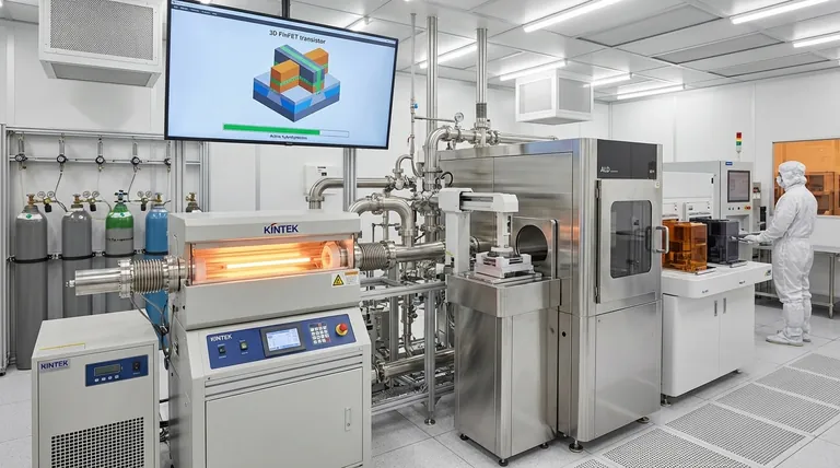
Fabricating Complex 3D Nanostructures
This integrated approach moves device fabrication from two dimensions into three. By combining deposition and patterning in a single, controlled environment, you can build up complex, multi-material architectures.
This is essential for next-generation devices like advanced 3D transistors (FinFETs), micro-electro-mechanical systems (MEMS), and complex photonic circuits.
Understanding the Trade-offs and Challenges
While powerful, integration introduces its own set of considerations that must be managed for a successful implementation.
Increased System Complexity
An integrated system is inherently more complex than its standalone components. This leads to a higher initial capital investment, a larger physical footprint, and more demanding maintenance protocols.
Process Interdependence
In a tightly integrated workflow, a failure in one module can halt the entire fabrication line. This contrasts with a siloed approach where other processes can continue if one tool is down for maintenance.
Throughput vs. Capability
The primary goal of integration is often to enable novel capabilities or achieve ultimate precision, which may come at the expense of raw throughput. A balance must be struck between the need for advanced device architecture and the demand for high-volume production.
Making the Right Choice for Your Goal
The decision to pursue an integrated CVD system should be driven by your ultimate fabrication objective.
- If your primary focus is pushing device performance limits: Integrate CVD with ALD to create novel heterostructures with atomically sharp interfaces for next-generation electronics.
- If your primary focus is high-resolution, dense patterning: Integrate CVD with nanoimprint or e-beam lithography to fabricate complex photonic devices or advanced logic circuits with minimal defects.
- If your primary focus is accelerating research and development: An integrated cluster tool allows for the rapid prototyping of new device concepts and material stacks in a single, controlled vacuum environment.
Ultimately, integrating your CVD furnace transforms it from a simple deposition tool into the versatile core of a multi-functional fabrication platform.
Summary Table:
| Integration Type | Key Benefits | Ideal Applications |
|---|---|---|
| CVD + ALD | Atomic-level precision, sharp interfaces | Next-gen electronics, heterostructures |
| CVD + NIL | High-resolution patterning, reduced defects | Photonic devices, logic circuits |
| CVD in Cluster Tools | Rapid prototyping, unified workflow | R&D, 3D nanostructures |
Ready to elevate your device fabrication with integrated solutions? KINTEK specializes in advanced high-temperature furnaces, including CVD tube furnaces, Muffle, Tube, Rotary Furnaces, Vacuum & Atmosphere Furnaces, and CVD/PECVD Systems. Leveraging our exceptional R&D and in-house manufacturing, we offer deep customization to precisely meet your unique experimental needs. Contact us today to discuss how our tailored solutions can enhance your lab's precision and efficiency!
Visual Guide

Related Products
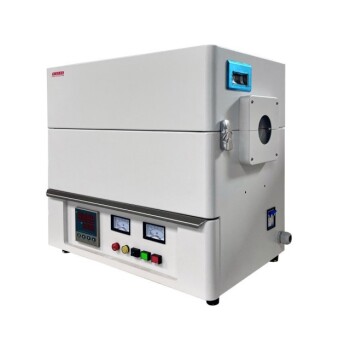
- Custom Made Versatile CVD Tube Furnace Chemical Vapor Deposition CVD Equipment Machine
- Split Chamber CVD Tube Furnace with Vacuum Station CVD Machine
- Multi Heating Zones CVD Tube Furnace Machine for Chemical Vapor Deposition Equipment
- Slide PECVD Tube Furnace with Liquid Gasifier PECVD Machine
- Inclined Rotary Plasma Enhanced Chemical Deposition PECVD Tube Furnace Machine
People Also Ask
- Why are CVD tube furnace sintering systems indispensable for 2D material research and production? Unlock Atomic-Scale Precision
- Which industries and research fields benefit from CVD tube furnace sintering systems for 2D materials? Unlock Next-Gen Tech Innovations
- How might AI and machine learning enhance CVD tube furnace processes? Boost Quality, Speed, and Safety
- How does CVD tube furnace sintering enhance graphene growth? Achieve Superior Crystallinity and High Electron Mobility
- What is a CVD tube furnace and what is its primary function? Discover Precision Thin-Film Deposition