At its core, Chemical Vapor Deposition (CVD) is the foundational technology that allows for the precise, layer-by-layer construction of modern CMOS transistors. Its importance stems from its unparalleled ability to deposit a wide variety of high-quality, uniform films—from insulators (dielectrics) to conductors—which serve as the essential building blocks for these microscopic electronic switches. Without CVD, the intricate, multi-layered architecture of a modern processor would be impossible to fabricate.
The true value of CVD isn't just its ability to deposit many materials, but its unique capacity to create highly conformal layers. This ensures complete, uniform coverage over the increasingly complex 3D topographies of modern chips, a feat that alternative methods struggle to achieve.
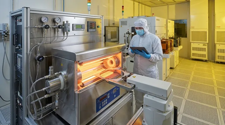
The Role of CVD in Building a Transistor
A CMOS transistor is not a monolithic block but a carefully assembled stack of different material layers. CVD is the primary method used to create many of these critical layers with the required purity and structural integrity.
Depositing Critical Dielectric (Insulating) Layers
Every transistor needs perfect insulators to direct the flow of electricity and prevent short circuits. CVD excels at creating these dielectric films.
Common examples include Silicon Dioxide (SiO₂) and Silicon Nitride (Si₃N₄). These are used for gate insulation, isolating conductive layers from one another, and creating a protective final "passivation" layer over the chip. The quality of these films is paramount; they must be dense and free of pinholes to prevent current leakage.
Forming Conductive Layers and Interconnects
While copper is used for the main wiring, CVD is critical for creating other conductive structures, especially those within tight, vertical spaces.
A key material is Tungsten (W). CVD is used to completely fill microscopic vertical holes, called contacts and vias, that connect different layers of the chip's circuitry. This process, known as creating a "tungsten plug," ensures a reliable electrical path between layers.
CVD is also used to deposit polycrystalline silicon (polysilicon), which has historically been the primary material for the transistor's gate electrode—the "switch" that turns the transistor on and off.
Growing High-Purity Semiconductor Films
Beyond just depositing materials on a surface, certain CVD processes can grow perfect, single-crystal films that mimic the underlying silicon wafer. This is called epitaxy.
Epitaxial growth is used to create the ultra-pure, defect-free transistor channel where electrons flow. It is also used to create strained silicon, a technique where the silicon lattice is intentionally stretched to allow electrons to move faster, directly boosting the processor's speed.
The Key Advantage: Conformality
As transistors shrink, their geometry becomes taller and more complex, with deep trenches and vertical fins (as in FinFET architectures). Covering these 3D surfaces evenly is a major fabrication challenge.
Why CVD Excels on 3D Structures
CVD is a chemical process where precursor gases are introduced into a chamber and react on the wafer's hot surface to form the desired film. Because the deposition is driven by a chemical reaction rather than a physical line-of-sight spray, the film grows on all exposed surfaces simultaneously.
This results in a highly conformal coating, meaning the film has a uniform thickness on the top, bottom, and vertical sidewalls of any feature. This property is also known as good step coverage.
The Limitation of Alternative Methods
This contrasts sharply with methods like Physical Vapor Deposition (PVD), or sputtering. PVD acts more like spray-painting, bombarding a target to eject atoms that then coat the wafer.
This line-of-sight process struggles with complex topography. It deposits a thick layer on top surfaces but a much thinner, weaker layer on the sidewalls and bottom of a trench, leading to voids, gaps, and potential device failure.
Understanding the Trade-offs
While indispensable, CVD is not the only deposition technique, and it comes with its own set of challenges. Understanding these trade-offs clarifies why it's chosen for specific, critical steps.
CVD vs. PVD
The primary trade-off is conformality versus simplicity. CVD provides superior film quality and the conformality needed for complex structures. PVD is often a simpler, faster, and lower-temperature process, making it suitable for less-demanding applications like depositing metal layers that don't need to fill deep trenches.
Process Complexity and Safety
CVD systems are complex and often operate at high temperatures and under vacuum. Furthermore, the precursor gases used (like silane or tungsten hexafluoride) can be highly toxic, flammable, or corrosive, requiring significant investment in safety and handling infrastructure.
Film Purity and Stress
The chemical nature of CVD means that byproducts from the reaction or unreacted precursors can become trapped in the film as impurities. Additionally, the deposited film can have internal stress, which, if not managed, can cause the film to crack or deform the wafer.
How CVD Aligns with Core Fabrication Goals
Choosing a deposition method depends entirely on the specific goal for that layer in the device.
- If your primary focus is device performance and scaling: CVD is non-negotiable for depositing the ultra-thin, high-k gate dielectrics and creating the strained silicon channels needed for faster, more efficient transistors.
- If your primary focus is manufacturing yield and reliability: CVD's superior conformality is essential for void-free filling of interconnects and ensuring complete electrical isolation between components, which directly reduces defects and chip failures.
- If your primary focus is material innovation: The flexibility of CVD allows for the integration of novel materials, such as 2D materials or new dielectrics, which is key to developing the next generation of semiconductor technology.
Ultimately, mastering Chemical Vapor Deposition is synonymous with mastering the art of modern semiconductor fabrication.
Summary Table:
| Aspect | Role of CVD in CMOS Devices |
|---|---|
| Dielectric Layers | Deposits insulators like SiO₂ and Si₃N₄ for gate insulation and isolation, preventing current leakage. |
| Conductive Layers | Forms tungsten plugs and polysilicon gates for reliable interconnects and switching. |
| Semiconductor Films | Grows epitaxial layers for high-purity channels and strained silicon to enhance electron mobility. |
| Conformality | Ensures uniform film coverage on 3D structures like trenches and fins, critical for modern chip architectures. |
| Advantages | Superior step coverage, material versatility, and support for device scaling and innovation. |
Unlock the Full Potential of Your Semiconductor Fabrication with KINTEK
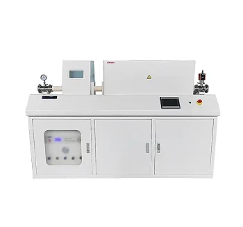
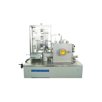
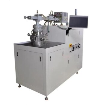
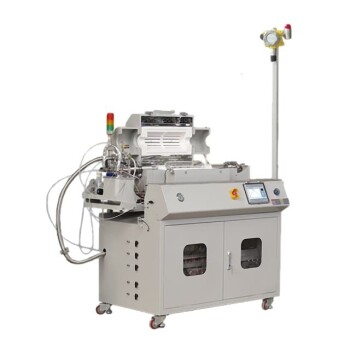
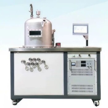
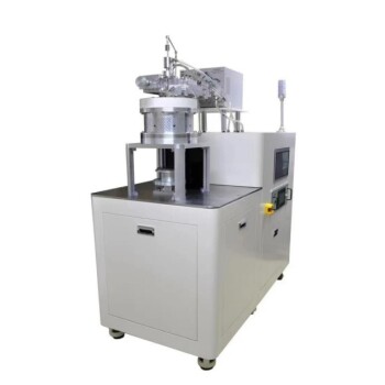
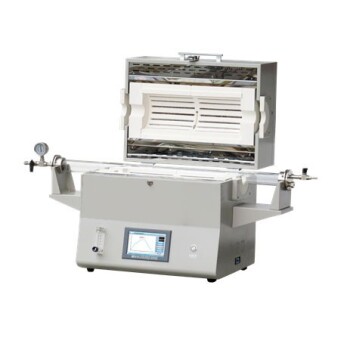
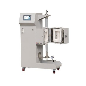
Leveraging exceptional R&D and in-house manufacturing, KINTEK provides diverse laboratories with advanced high-temperature furnace solutions. Our product line, including Muffle, Tube, Rotary Furnaces, Vacuum & Atmosphere Furnaces, and CVD/PECVD Systems, is complemented by our strong deep customization capability to precisely meet unique experimental requirements. Whether you're focused on enhancing device performance, improving manufacturing yield, or pioneering material innovations, our tailored CVD systems deliver the precision and reliability you need for cutting-edge CMOS development.
Contact us today to discuss how we can support your specific fabrication goals and drive your research forward!
Visual Guide

Related Products
- Slide PECVD Tube Furnace with Liquid Gasifier PECVD Machine
- RF PECVD System Radio Frequency Plasma Enhanced Chemical Vapor Deposition
- Inclined Rotary Plasma Enhanced Chemical Deposition PECVD Tube Furnace Machine
- Inclined Rotary Plasma Enhanced Chemical Deposition PECVD Tube Furnace Machine
- Cylindrical Resonator MPCVD Machine System for Lab Diamond Growth
People Also Ask
- What are the classifications of CVD based on vapor characteristics? Optimize Your Thin Film Deposition Process
- Why are high-purity quartz boats used for graphene oxide reduction? Ensure Chemical Purity & Thermal Stability
- Why is a high vacuum diffusion pump system required when preparing Ge-Se-Te-In reaction materials? Ensure Peak Purity
- How does chemical vapour deposition (CVD) differ from PVD? Key Differences in Thin-Film Coating Methods
- How is silicon dioxide deposited from tetraethylorthosilicate (TEOS) in PECVD? Achieve Low-Temperature, High-Quality SiO2 Films
