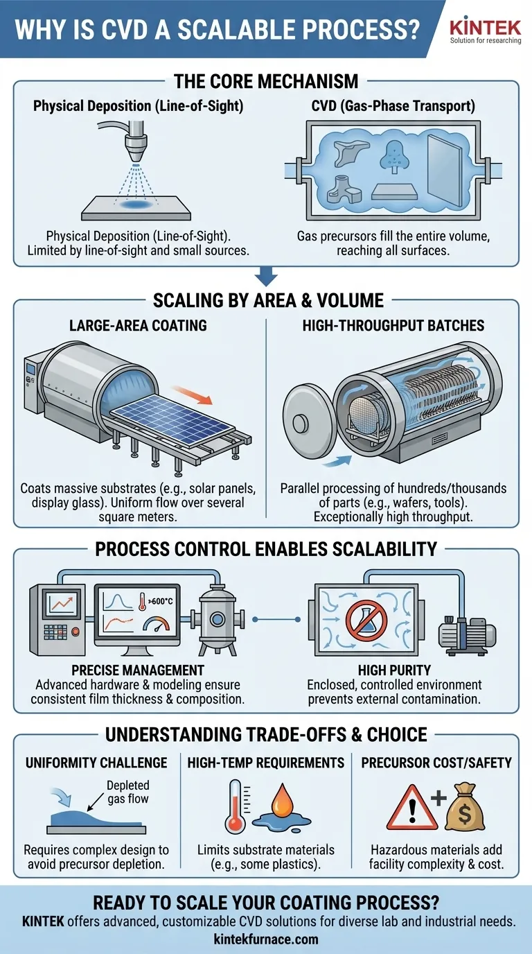
At its core, Chemical Vapor Deposition (CVD) is considered a scalable process because its fundamental mechanism is not constrained by line-of-sight or small point sources. The use of gaseous chemical precursors allows the process to efficiently coat large surface areas and large batches of components simultaneously, making it highly adaptable from laboratory-scale experiments to high-volume industrial production.
The scalability of CVD stems from its gas-phase nature. Unlike processes that spray material from a single point, CVD precursors fill the entire reactor, enabling uniform and high-purity coatings across vast areas or numerous parts in a single run.
The Mechanics of CVD Scalability
To understand why CVD scales effectively, we must look at how the material is transported and deposited. The process is fundamentally different from physical deposition methods, which directly influences its production capabilities.
Uniform Deposition via Gas-Phase Transport
The defining feature of CVD is the use of volatile precursor gases. These gases are introduced into a reaction chamber where they decompose or react on a heated substrate surface, forming a solid film.
Because the precursors exist as a gas, they naturally expand to fill the entire volume of the reactor. This allows them to reach all exposed surfaces of the substrate, including complex shapes and the surfaces of many individual parts arranged in a batch.
Scaling by Area: Coating Large Substrates
For applications like solar panels, architectural glass, or display manufacturing, the ability to coat a single, large surface is paramount.
CVD reactors can be designed to be very large, accommodating massive substrates. The gas delivery system is engineered to ensure a uniform flow and concentration of precursors across the entire surface, enabling consistent film thickness and properties over areas of several square meters.
Scaling by Volume: High-Throughput Batch Processing
For smaller components, such as semiconductor wafers, cutting tools, or medical implants, scalability is achieved through batch processing.
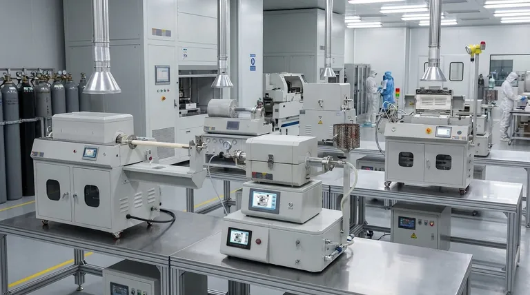
Hundreds or even thousands of parts can be loaded into a large CVD furnace. The precursor gases flow around and between each component, depositing a uniform coating on all of them simultaneously. This parallel processing results in exceptionally high throughput.
How Process Control Enables Scalability
Simply making a reactor bigger is not enough. The scalability of CVD is only successful because the process parameters can be precisely managed, ensuring that quality and uniformity are not sacrificed for volume.
Maintaining Film Uniformity
The primary challenge in scaling CVD is maintaining consistent film thickness and composition. As reactor size or batch load increases, factors like gas flow dynamics and temperature gradients become more complex.
Modern CVD systems use sophisticated computer modeling and advanced hardware to control gas injection, chamber pressure, and multi-zone heating. This precise control ensures that all surfaces—whether on a single large substrate or across a thousand small parts—experience the same deposition conditions.
Ensuring High Purity at Scale
CVD is an enclosed, high-vacuum or controlled-atmosphere process. This prevents contaminants from the outside environment from being incorporated into the film.
This inherent cleanliness is maintained even in large-scale systems. The ability to produce high-purity films consistently across large batches is a critical reason why CVD is the dominant technology in industries like microelectronics.
Understanding the Trade-offs
While highly scalable, CVD is not without its challenges. Acknowledging these limitations is key to making an informed decision.
The Challenge of Uniformity
Achieving perfect uniformity in a large or densely packed reactor is a significant engineering challenge. Precursor gases can become depleted as they flow over surfaces, leading to thinner coatings downstream. This requires complex reactor design and process tuning to mitigate.
High-Temperature Requirements
Many CVD processes operate at very high temperatures (often >600°C). This can limit the types of substrate materials that can be used, as some plastics or low-melting-point metals cannot withstand the heat.
Precursor Cost and Safety
The chemical precursors used in CVD can be expensive, toxic, corrosive, or flammable. Scaling up the process means scaling up the storage and handling of these hazardous materials, which adds significant cost and complexity to the required facility infrastructure.
Making the Right Choice for Your Application
Choosing CVD must be a strategic decision based on your specific production goals and material constraints.
- If your primary focus is large-area coatings (e.g., solar panels, flat-panel displays): CVD is a leading choice due to its proven ability to deposit uniform, high-performance films over vast surfaces.
- If your primary focus is high-volume production of smaller components (e.g., semiconductor wafers, machine tools): CVD's batch processing capability offers unmatched throughput and cost-effectiveness at scale.
- If your primary focus is coating temperature-sensitive materials: You must explore lower-temperature variants like Plasma-Enhanced CVD (PECVD) or accept the limitations of the traditional thermal process.
Understanding these principles of scalability allows you to leverage CVD not just as a deposition technique, but as a strategic manufacturing solution.
Summary Table:
| Aspect | Key Points |
|---|---|
| Scalability | Adaptable from lab to industrial scale; efficient for large areas and batch processing. |
| Mechanism | Gas-phase precursors fill reactor, allowing uniform deposition on complex shapes and multiple parts. |
| Control | Precise management of gas flow, temperature, and pressure ensures consistency and high purity. |
| Challenges | Uniformity issues, high temperatures, and precursor cost/safety require careful engineering. |
Ready to Scale Your Coating Processes with Advanced CVD Solutions? Leveraging exceptional R&D and in-house manufacturing, KINTEK provides diverse laboratories with advanced high-temperature furnace solutions. Our product line, including Muffle, Tube, Rotary Furnaces, Vacuum & Atmosphere Furnaces, and CVD/PECVD Systems, is complemented by our strong deep customization capability to precisely meet unique experimental requirements. Whether you're in microelectronics, solar, or tool manufacturing, we deliver scalable, high-purity coatings tailored to your needs. Contact us today to discuss how our CVD systems can boost your production efficiency and quality!
Visual Guide
Related Products
- Custom Made Versatile CVD Tube Furnace Chemical Vapor Deposition CVD Equipment Machine
- Split Chamber CVD Tube Furnace with Vacuum Station CVD Machine
- Multi Heating Zones CVD Tube Furnace Machine for Chemical Vapor Deposition Equipment
- Slide PECVD Tube Furnace with Liquid Gasifier PECVD Machine
- Inclined Rotary Plasma Enhanced Chemical Deposition PECVD Tube Furnace Machine
People Also Ask
- How can integrating CVD tube furnaces with other technologies benefit device fabrication? Unlock Advanced Hybrid Processes
- Why are CVD tube furnace sintering systems indispensable for 2D material research and production? Unlock Atomic-Scale Precision
- How might AI and machine learning enhance CVD tube furnace processes? Boost Quality, Speed, and Safety
- What improvements can be made to the bonding force of gate dielectric films using a CVD tube furnace? Enhance Adhesion for Reliable Devices
- How does CVD tube furnace sintering enhance graphene growth? Achieve Superior Crystallinity and High Electron Mobility


