The 500 °C annealing furnace is the fundamental catalyst that transforms electrospun precursor fibers into functional, high-performance semiconducting nanowires. It provides the thermal energy required to execute two critical transitions: the chemical decomposition of non-conductive organic "template" materials and the physical crystallization of the metal oxide semiconductors. Without this precise thermal environment, the material would lack the crystalline structure and electronic properties necessary to operate as a field-effect transistor (FET).
Core Takeaway: A 500 °C annealing process is required to achieve the pyrolysis of polymer matrices and the crystallization of metal salts into an $\text{In}2\text{O}3@\text{ZnO}$ heterojunction. This specific temperature ensures high carrier mobility and a superior $I{\text{on}}/I{\text{off}}$ ratio by optimizing the material's purity and crystal quality.
Chemical Transformation and Purification
Pyrolysis of the Polymer Matrix
The electrospinning process uses a polymer matrix to hold metal salts in a nanowire shape. The 500 °C furnace environment triggers pyrolysis, which oxidizes and removes this organic binder.
This step is vital because any residual carbon or polymer would act as an insulator. Removing these impurities is the first step in creating a conductive path for electrons.
Thermal Decomposition of Metal Salts
At 500 °C, metal salt precursors undergo a chemical transition into their oxide forms ($\text{In}_2\text{O}_3$ and $\text{ZnO}$). This solid-state reaction converts the material from a chemical mixture into a semiconducting oxide.
The furnace provides the specific thermal gradient needed for the dehydration and lattice reorganization of precursors like $\text{InOOH}$. This ensures the final material reaches a chemically stable state.
Structural Optimization and Interface Engineering
Achieving High Crystallinity
High-temperature treatment is essential for inducing an ordered atomic structure. In the furnace, grain growth is promoted, transforming the material from an amorphous state into a highly crystalline wurtzite or cubic structure.
Superior crystallinity reduces the number of grain boundaries and defects. This leads to enhanced carrier mobility, allowing electrons to move more freely through the nanowire.
Formation of the Ring Heterojunction
The 500 °C environment is specifically calibrated to form a stable ring heterojunction interface between the $\text{In}_2\text{O}_3$ and $\text{ZnO}$ layers. This interface is the heart of the transistor's switching capability.
A well-defined heterojunction allows for efficient charge separation and transport. This directly optimizes the $I_{\text{on}}/I_{\text{off}}$ ratio, ensuring the transistor can switch between "on" and "off" states with high precision.
Performance Tuning through Thermal Control
Regulation of Oxygen Vacancy Defects
The annealing temperature and atmosphere within the furnace effectively control the concentration of oxygen vacancy defects. These vacancies act as charge carriers in n-type metal oxides.
By precisely maintaining 500 °C, manufacturers can tune the resistive switching characteristics of the material. This creates a balance between conductivity and the ability to control current via the gate voltage.
Morphological Control and Aspect Ratio
Using a high-temperature furnace allows for a programmed heating rate (such as 2 °C/min). This slow ramp-up regulates the rates of crystal nucleation and growth.
Controlled heating induces anisotropic growth, resulting in nanowires with high aspect ratios. This maximizes the specific surface area, which is vital for charge transfer efficiency and sensor sensitivity.
Understanding the Trade-offs
The Risk of Grain Overgrowth
While high temperatures are necessary for crystallinity, exceeding the optimal temperature can lead to excessive grain growth. This may cause the nanowires to become brittle or create large grain boundaries that scatter charge carriers.
Substrate Compatibility and Stress
Operating at 500 °C limits the choice of substrates to materials that can withstand high heat, such as silicon or specialized glass. Additionally, rapid cooling from these temperatures can introduce internal residual stresses that may lead to film cracking or delamination.
Making the Right Choice for Your Manufacturing Goal
How to Apply This to Your Process
To optimize the manufacturing of $\text{In}_2\text{O}_3@\text{ZnO}$ nanowire transistors, consider the following technical priorities:
- If your primary focus is Maximum Electron Mobility: Ensure the furnace maintains a highly uniform thermal field at 500 °C to promote the highest possible crystallinity and minimize lattice defects.
- If your primary focus is Device Reproducibility: Utilize a furnace with precise heating rate control (e.g., 2 °C/min) to standardize the nucleation process across different batches.
- If your primary focus is Power Efficiency ($I_{\text{on}}/I_{\text{off}}$ ratio): Carefully regulate the annealing atmosphere (oxygen vs. inert gas) at 500 °C to fine-tune the oxygen vacancy concentration.
By mastering the thermal environment of the annealing furnace, you ensure the transition from a simple chemical precursor to a sophisticated, high-performance electronic component.
Summary Table:
| Process Step | Material Transformation | Performance Benefit |
|---|---|---|
| Pyrolysis | Removes organic binders/impurities | Creates clean conductive paths |
| Decomposition | Converts metal salts to oxides | Forms the semiconducting base |
| Crystallization | Promotes ordered grain growth | Increases carrier mobility |
| Heterojunction | Develops stable ring interface | Optimizes $I_{\text{on}}/I_{\text{off}}$ ratio |
| Defect Control | Regulates oxygen vacancies | Tunes resistive switching |
Elevate Your Nanowire Research with KINTEK Precision
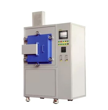
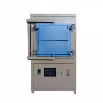
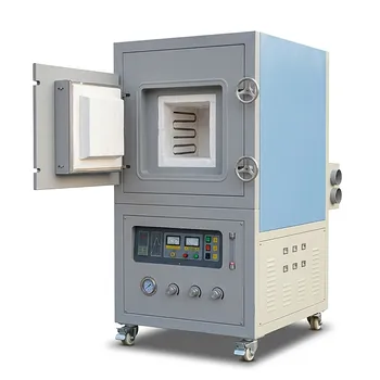
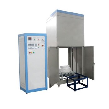
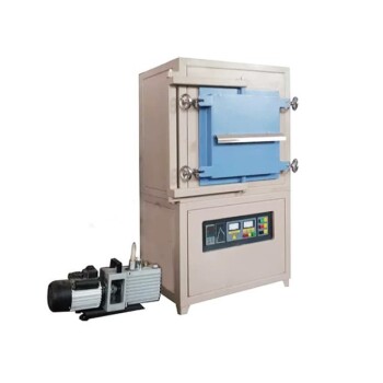
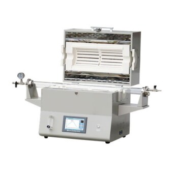
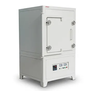
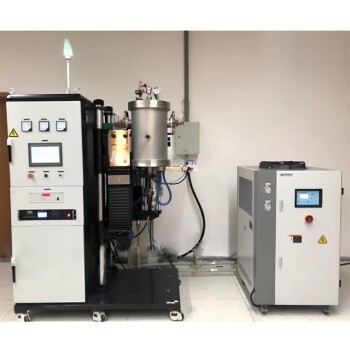
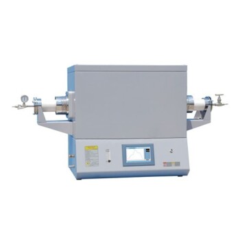
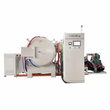
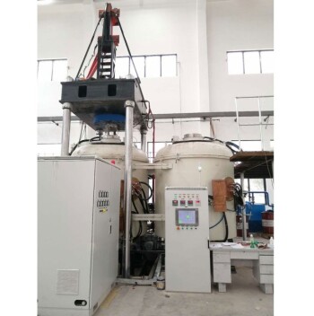
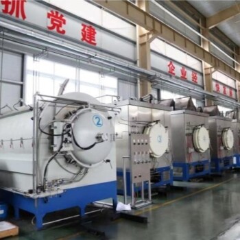
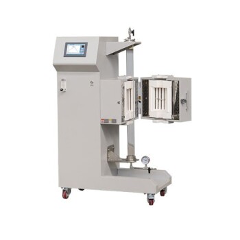
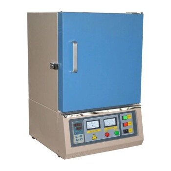
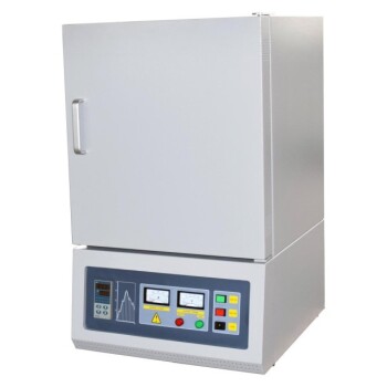
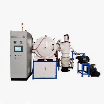
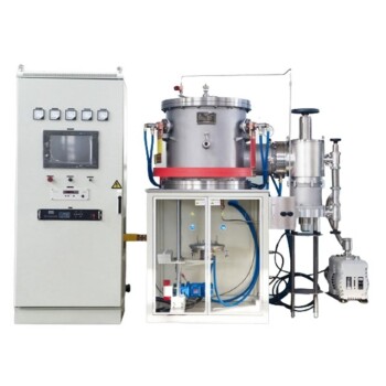
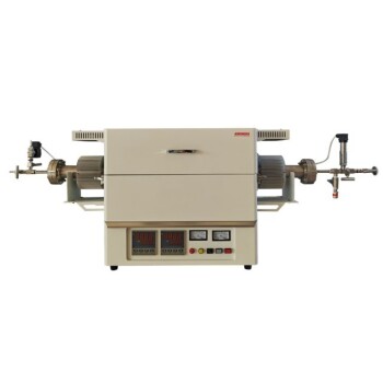
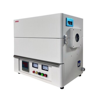
Achieving the perfect 500 °C thermal environment is critical for high-performance $\text{In}_2\text{O}_3@\text{ZnO}$ heterojunctions. KINTEK specializes in advanced laboratory equipment, offering a comprehensive range of high-temperature furnaces—including muffle, tube, rotary, vacuum, CVD, and atmosphere furnaces—engineered to provide the precise ramp rates (e.g., 2 °C/min) and thermal uniformity your process demands.
Whether you need to optimize carrier mobility or fine-tune oxygen vacancy defects, our systems are fully customizable to meet your unique semiconductor manufacturing requirements.
Ready to enhance your lab's efficiency? Contact our technical experts today to find the ideal furnace solution for your next breakthrough.
References
- Bo He, Shouguo Wang. Electrospun Coaxial Nanowire‐Based FETs with Annular Heterogeneous Interface Gain for Intelligent Functional Electronics. DOI: 10.1002/adfm.202316375
This article is also based on technical information from Kintek Furnace Knowledge Base .
Related Products
- Controlled Inert Nitrogen Hydrogen Atmosphere Furnace
- 1400℃ Controlled Inert Nitrogen Atmosphere Furnace
- High Temperature Muffle Oven Furnace for Laboratory Debinding and Pre Sintering
- Laboratory Muffle Oven Furnace with Bottom Lifting
- 1700℃ Controlled Inert Nitrogen Atmosphere Furnace
People Also Ask
- How does hydrogen furnace annealing assist in preparing mechanically alloyed powders for compaction?
- How does atmospheric annealing in a controlled hydrogen furnace affect the cold compaction behavior of metal powders?
- What are the characteristics and uses of hydrogen atmospheres in furnaces? Unlock Clean Metal Processing
- What are the characteristics and uses of hydrogen atmosphere in furnaces? Achieve Superior Surface Purity and Bonding
- What controlled-atmosphere furnace conditions are required for sintering powder metallurgy copper alloy compacts? Ideal Setup