At their core, Chemical Vapor Deposition (CVD) furnaces are indispensable because they allow us to build high-performance materials from the atom up. This process enables the creation of exceptionally pure, uniform, and durable thin films and coatings that are foundational to modern technology, from microchips to solar panels.
The true value of a CVD furnace is not merely in applying a coating, but in its unique ability to precisely construct a new material layer on a substrate, granting it properties that are often impossible to achieve through any other manufacturing method.
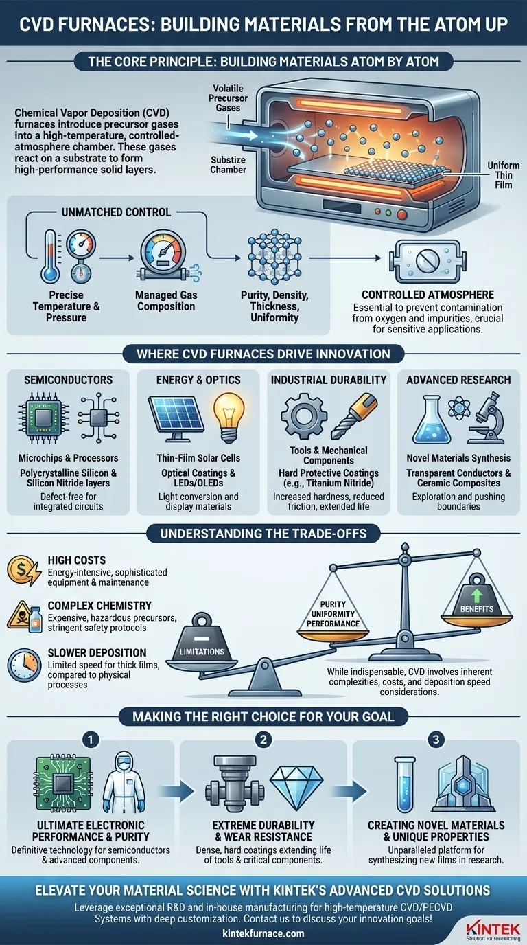
The Core Principle: Building Materials Atom by Atom
CVD is a transformative technology because it operates at the most fundamental level of material creation. This control is what sets it apart.
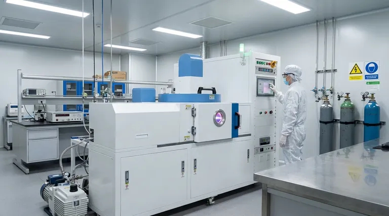
What is Chemical Vapor Deposition (CVD)?
In a CVD furnace, volatile precursor gases are introduced into a high-temperature, controlled-atmosphere chamber. These gases react or decompose on the surface of a substrate, depositing a solid, thin film of the desired material.
The process is analogous to steam condensing into ice on a cold window, but instead of water, it involves complex chemical reactions that form highly engineered solid layers.
Unmatched Control Over Material Properties
This atomic-level deposition allows for extreme precision. By carefully managing temperature, pressure, and gas composition, we can dictate the final material's purity, density, thickness, and uniformity.
This level of control is critical for creating materials with enhanced mechanical, electrical, or optical properties that are far superior to the underlying substrate.
The Power of a Controlled Atmosphere
CVD furnaces typically operate under vacuum or a strictly controlled atmosphere. This environment is essential for preventing contamination from oxygen and other atmospheric gases.
Without this control, impurities would be incorporated into the film, creating defects that would compromise the performance and integrity of the final product, especially in sensitive applications like semiconductors.
Where CVD Furnaces Drive Innovation
The versatility and precision of CVD make it a cornerstone technology across numerous high-stakes industries, enabling products and capabilities that define the modern world.
In the Semiconductor Industry
Virtually every modern microchip, processor, and memory device relies on CVD. It is used to deposit the ultra-pure, defect-free layers of materials like polycrystalline silicon and silicon nitride that form the transistors and insulating layers at the heart of integrated circuits.
In Energy and Optics
CVD is essential for manufacturing thin-film solar cells, where it is used to create the light-absorbing layers that convert sunlight into electricity. It is also used to produce high-performance optical coatings and is critical in fabricating the materials used in LEDs and OLEDs for displays and lighting.
For Industrial Durability
For tools, molds, and mechanical components that face extreme wear, CVD provides exceptionally hard and protective coatings. These layers, often made of materials like titanium nitride, dramatically increase surface hardness, reduce friction, and prevent corrosion, extending the life of the part.
In Advanced Research
For materials scientists and nanotechnologists, CVD furnaces are invaluable research platforms. Their flexibility allows for the exploration and synthesis of novel materials, from new types of transparent conductors to advanced ceramic composites, pushing the boundaries of what is possible.
Understanding the Trade-offs
While indispensable, the CVD process has inherent complexities and limitations that must be considered.
High Energy and Equipment Costs
CVD furnaces require high temperatures and often a high-vacuum environment to function correctly. This makes the process energy-intensive and requires sophisticated, expensive equipment and maintenance.
Complex Precursor Chemistry
The success of a CVD process is entirely dependent on the precursor gases used. These chemicals can be expensive, hazardous, or difficult to handle, requiring stringent safety protocols and supply chain management. The chemistry must be perfectly matched to the desired film and substrate.
Deposition Rate Limitations
While incredibly precise, CVD can be a slower deposition method compared to physical processes like sputtering, especially for thicker films. This can be a limiting factor in high-volume, low-cost manufacturing where speed is a primary concern.
Making the Right Choice for Your Goal
The decision to use CVD is driven by an uncompromising need for material performance.
- If your primary focus is ultimate electronic performance and purity: CVD is the definitive technology for creating the foundational layers of semiconductors and advanced electronic components.
- If your primary focus is extreme durability and wear resistance: CVD provides dense, hard coatings that significantly extend the life and performance of tools and critical components.
- If your primary focus is creating novel materials with unique properties: The versatility of the CVD process makes it an unparalleled platform for synthesizing new films and nanostructures in a research setting.
Ultimately, the power of a CVD furnace lies in its ability to transform simple gases into a complex, solid, and highly-engineered material, one atom at a time.
Summary Table:
| Aspect | Details |
|---|---|
| Core Principle | Builds materials atom by atom using chemical vapor deposition in controlled environments. |
| Key Advantages | Unmatched purity, uniformity, and durability of thin films; precise control over material properties. |
| Applications | Semiconductors, solar cells, optical coatings, wear-resistant tools, and advanced research. |
| Limitations | High energy costs, complex precursor chemistry, and slower deposition rates for thick films. |
Elevate your material science projects with KINTEK's advanced CVD furnace solutions! Leveraging exceptional R&D and in-house manufacturing, we provide high-temperature furnaces like CVD/PECVD Systems with deep customization to meet your unique experimental needs. Whether you're in semiconductors, energy, or research, our technology ensures precise, high-performance results. Contact us today to discuss how we can support your innovation goals!
Visual Guide
Related Products
- Custom Made Versatile CVD Tube Furnace Chemical Vapor Deposition CVD Equipment Machine
- Split Chamber CVD Tube Furnace with Vacuum Station CVD Machine
- Multi Heating Zones CVD Tube Furnace Machine for Chemical Vapor Deposition Equipment
- Slide PECVD Tube Furnace with Liquid Gasifier PECVD Machine
- Controlled Inert Nitrogen Hydrogen Atmosphere Furnace
People Also Ask
- What temperature range do standard CVD tube furnaces operate at? Unlock Precision for Your Material Deposition
- What are the benefits of developing new precursor materials for CVD tube furnaces? Unlock Advanced Thin-Film Synthesis
- What are the key application fields of CVD tube furnaces? Unlock Precision in Thin-Film Synthesis
- Which industries and research fields benefit from CVD tube furnace sintering systems for 2D materials? Unlock Next-Gen Tech Innovations
- Why are CVD tube furnace sintering systems indispensable for 2D material research and production? Unlock Atomic-Scale Precision


