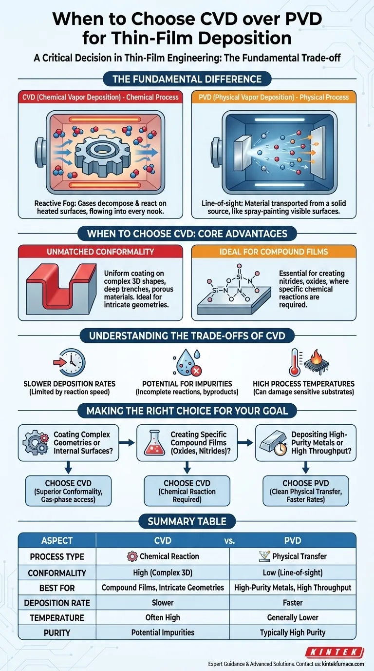
Choosing between CVD and PVD is a critical decision in thin-film engineering. Chemical Vapor Deposition (CVD) should be your choice when you need to coat complex, three-dimensional surfaces or when depositing specific compound materials like nitrides and oxides. Unlike the line-of-sight nature of Physical Vapor Deposition (PVD), the gas-phase chemical reactions in CVD allow it to create highly conformal films that uniformly cover intricate geometries.
The decision ultimately hinges on a fundamental trade-off. CVD excels at providing superior conformality for complex shapes due to its chemical reaction-based process. In contrast, PVD is often preferred for its ability to deposit high-purity films, especially metals, at a faster rate through a direct physical transfer.
The Fundamental Difference: Chemical vs. Physical
To make an informed choice, you must first understand how each process works at a foundational level. The names themselves reveal the core distinction.
How Chemical Vapor Deposition (CVD) Works
CVD is a chemical process. It involves introducing one or more volatile precursor gases into a reaction chamber.
These gases decompose and react on the surface of the heated substrate, forming the desired solid material as a thin film. Think of it as "painting with a reactive fog" that can flow into and coat every nook and cranny.
How Physical Vapor Deposition (PVD) Works
PVD is a physical process. It involves transporting material from a solid source (the "target") to the substrate in a vacuum environment.
This is typically done by vaporizing the source material through methods like sputtering or evaporation. This process is line-of-sight, much like spray-painting, where the coating only deposits on surfaces directly visible to the source.
When to Choose CVD: Core Advantages
CVD's unique mechanism gives it distinct advantages in specific scenarios.
Unmatched Conformality
Because the deposition occurs from a gas phase, CVD can coat all surfaces of a substrate uniformly, regardless of its shape. This makes it the ideal choice for coating complex 3D objects, deep trenches, or porous materials where a line-of-sight process like PVD would fail.
Ideal for Compound Films
CVD is often the superior, or only, method for creating certain types of films. The process is perfectly suited for depositing compounds like nitrides (e.g., silicon nitride) and oxides (e.g., silicon dioxide), where specific chemical reactions are required to form the film.
Understanding the Trade-offs of CVD
No process is without its limitations. Being aware of CVD's trade-offs is crucial for avoiding costly mistakes.
Slower Deposition Rates
CVD processes are generally slower than PVD. The rate is limited by the speed of the surface chemical reactions, which can be a significant drawback for applications requiring high throughput or the rapid deposition of very thick films.
Potential for Impurities
The chemical reactions that define CVD can sometimes be incomplete or produce unwanted byproducts. These can become incorporated into the thin film as impurities, potentially affecting its performance and purity compared to films made with PVD.
High Process Temperatures
Many CVD processes require high substrate temperatures to initiate and sustain the necessary chemical reactions. This can damage heat-sensitive substrates, such as plastics or certain electronic components, making CVD unsuitable for those applications.
Making the Right Choice for Your Goal
Your application's primary goal should guide your decision. Use these guidelines to select the right process.
- If your primary focus is coating complex geometries or internal surfaces: Choose CVD for its superior conformality, as the gas-phase process can reach areas physically inaccessible to PVD.
- If your primary focus is depositing high-purity metals or achieving high throughput: Choose PVD for its clean, physical transfer mechanism and characteristically faster deposition rates.
- If your primary focus is creating specific compound films like oxides or nitrides: CVD is often the necessary choice, as its chemical reaction process is required to form these materials on the substrate.
Understanding this core distinction between a chemical reaction and a physical transfer empowers you to select the precise tool for your engineering goal.
Summary Table:
| Aspect | CVD (Chemical Vapor Deposition) | PVD (Physical Vapor Deposition) |
|---|---|---|
| Process Type | Chemical reaction-based | Physical transfer-based |
| Conformality | High, ideal for complex 3D shapes | Low, line-of-sight only |
| Best For | Compound films (e.g., nitrides, oxides), intricate geometries | High-purity metals, high throughput |
| Deposition Rate | Slower | Faster |
| Temperature | Often high, may damage sensitive substrates | Generally lower, more versatile |
| Purity | Potential for impurities from reactions | Typically high purity |
Need expert guidance on selecting the right high-temperature furnace for your thin-film deposition? Leveraging exceptional R&D and in-house manufacturing, KINTEK provides diverse laboratories with advanced solutions like CVD/PECVD Systems, Muffle, Tube, Rotary Furnaces, and Vacuum & Atmosphere Furnaces. Our strong deep customization capability ensures we precisely meet your unique experimental requirements. Contact us today to enhance your lab's efficiency and achieve superior results!
Visual Guide
Related Products
- HFCVD Machine System Equipment for Drawing Die Nano Diamond Coating
- Custom Made Versatile CVD Tube Furnace Chemical Vapor Deposition CVD Equipment Machine
- Inclined Rotary Plasma Enhanced Chemical Deposition PECVD Tube Furnace Machine
- 915MHz MPCVD Diamond Machine Microwave Plasma Chemical Vapor Deposition System Reactor
- Inclined Rotary Plasma Enhanced Chemical Deposition PECVD Tube Furnace Machine
People Also Ask
- What core function does CVD equipment serve in h-BN anti-corrosion? Master Precision Synthesis for High-Performance Films
- How can customers maximize the quality of CVD coatings? Master Pre-Coating Prep for Superior Results
- What is chemical vapor deposition (CVD) and its primary industrial application? Unlock Precision Thin Films for Electronics
- What is the significance of the vacuum pressure control system in the CVD coating process for powders?
- What is the function of high-purity Argon (Ar) gas during CVD? Optimize Your Thin Film Uniformity and Purity


