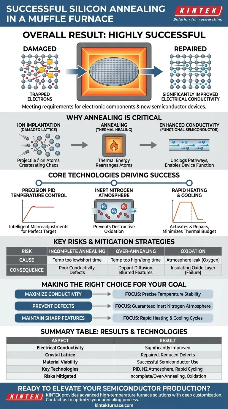
In short, the results were highly successful. The annealing process conducted in the muffle furnace significantly improved the silicon-based material's electrical conductivity. This enhancement was substantial enough to meet the demanding requirements for electronic component production, leading to the material's successful use in new semiconductor devices.
The core takeaway is that successful silicon annealing isn't merely about heating a material. It is a precise engineering process where the furnace's ability to control temperature and atmosphere directly dictates the final electrical properties and viability of the semiconductor.
Why Annealing is a Critical Step for Silicon
Annealing is a thermal treatment that fundamentally alters a material's physical and electrical properties. For silicon used in semiconductors, this step is not optional; it is essential for creating functional devices.
The Goal: Repairing the Crystal Lattice
Manufacturing processes, such as ion implantation (where atoms are fired into the silicon to change its conductivity), cause significant damage to silicon's highly ordered crystal structure. Annealing provides the thermal energy needed for atoms to rearrange themselves back into this perfect lattice structure, effectively healing the material.
The Outcome: Enhanced Electrical Conductivity
An ordered crystal lattice allows electrons to move through the material with minimal resistance. The damage from prior processing creates defects that trap these electrons, drastically reducing conductivity. By repairing the lattice, annealing removes these traps and "unclogs" the pathways for electricity, significantly improving conductivity.
The Application: Enabling Functional Semiconductors
This improved conductivity is the direct property that allows the material to function as a semiconductor. Without this step, the silicon would not possess the reliable electrical characteristics necessary to operate as a transistor, diode, or other electronic component.
The Core Technologies Driving Success
The positive results were not accidental. They were the direct outcome of specific technologies within the muffle furnace that provided an ideal environment for the process.
Precision Temperature Control (PID)
The furnace utilizes a PID (Proportional-Integral-Derivative) system for temperature control. Think of this as an exceptionally intelligent thermostat that doesn't just turn the heat on and off but constantly makes micro-adjustments to hit and maintain the exact target temperature without overshooting or undershooting. This precision is critical for repairing the lattice without melting or otherwise damaging the material.
Inert Atmosphere Control (Nitrogen)
At the high temperatures required for annealing, silicon reacts readily with oxygen, forming a layer of silicon dioxide (an insulator). This would destroy the material's conductive properties. The furnace floods the chamber with high-purity nitrogen gas, which displaces all the oxygen and provides an inert atmosphere, preventing this destructive oxidation.
Rapid Heating and Cooling
The ability to raise and lower the temperature quickly is key to maintaining the integrity of the crystal structure. A controlled, rapid thermal cycle activates the implanted atoms and repairs damage while minimizing the time the material spends at high temperatures. This prevents unwanted effects like dopant diffusion, which could blur the microscopic boundaries of the electronic components.
Understanding the Key Risks in Annealing
While powerful, annealing is a process with a narrow window for success. Failure to manage the key parameters can lead to a completely unusable product.
The Risk of Incomplete Annealing
If the temperature is too low or the duration is too short, the crystal lattice damage will not be fully repaired. This leaves behind residual defects that impede electron flow, resulting in poor conductivity and unreliable device performance.
The Problem of Over-Annealing
If the temperature is too high or held for too long, the carefully placed dopant atoms can begin to diffuse or move away from their intended positions. This blurring of microscopic junctions degrades the performance of the final transistor or device.
The Threat of Oxidation
Any failure in the atmosphere control system is catastrophic. Even a small leak that allows oxygen into the furnace chamber at high temperatures will lead to the formation of an insulating oxide layer, ruining the entire batch of material.
Making the Right Choice for Your Goal
To apply these principles, you must align your process control with your primary objective.
- If your primary focus is maximizing conductivity: Your priority must be precise temperature stability to ensure the crystal lattice is fully repaired.
- If your primary focus is preventing defects: You must guarantee the integrity and purity of the nitrogen atmosphere to eliminate any chance of oxidation.
- If your primary focus is maintaining sharp device features: You should leverage rapid heating and cooling cycles to minimize the total thermal budget and prevent dopant migration.
Ultimately, mastering the annealing process transforms a damaged material into a high-performance electronic component through precise, controlled thermal engineering.
Summary Table:
| Aspect | Result |
|---|---|
| Electrical Conductivity | Significantly improved, meeting requirements for electronic components |
| Crystal Lattice | Repaired, reducing defects and enabling electron flow |
| Material Viability | Successfully used in new semiconductor devices |
| Key Technologies | PID temperature control, inert nitrogen atmosphere, rapid thermal cycling |
| Risks Mitigated | Avoided incomplete annealing, over-annealing, and oxidation |
Ready to elevate your semiconductor production with precise annealing? KINTEK leverages exceptional R&D and in-house manufacturing to provide advanced high-temperature furnace solutions, including Muffle, Tube, Rotary Furnaces, Vacuum & Atmosphere Furnaces, and CVD/PECVD Systems. Our strong deep customization capability ensures we can precisely meet your unique experimental requirements, delivering enhanced electrical properties and reliability for your silicon-based materials. Contact us today to discuss how our tailored solutions can optimize your annealing process and drive innovation in your lab!
Visual Guide
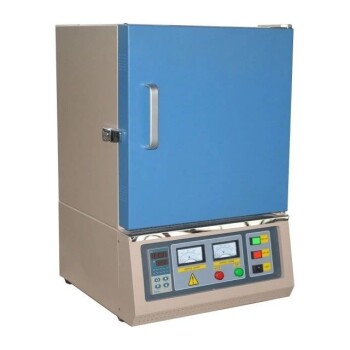
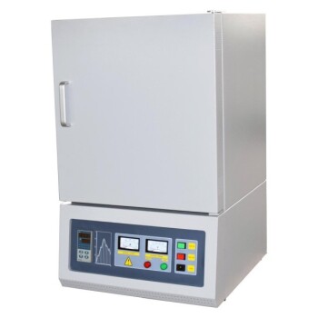
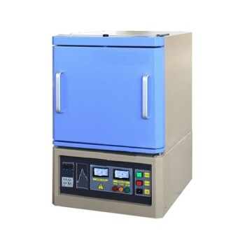
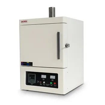
Related Products
- 1400℃ Muffle Oven Furnace for Laboratory
- 1700℃ High Temperature Muffle Oven Furnace for Laboratory
- 1800℃ High Temperature Muffle Oven Furnace for Laboratory
- 1200℃ Muffle Oven Furnace for Laboratory
- High Temperature Muffle Oven Furnace for Laboratory Debinding and Pre Sintering
People Also Ask
- What role does a muffle furnace play in refractory bricks? Enhance Performance and Durability Testing
- How is a laboratory high-temperature muffle furnace utilized in g-C3N4 synthesis? Optimize Your Thermal Polycondensation
- How is a laboratory muffle furnace used in 3D-printed PP-CF cross-linking? Achieve Thermal Stability at 150 °C
- What is the function of a laboratory muffle furnace in lignin determination? Precision Ashing for Biomass Analysis
- What role does a laboratory high-temperature muffle furnace play in the treatment of highly contaminated waste glass?