At its core, a Plasma-Enhanced Chemical Vapor Deposition (PECVD) system can deposit an exceptionally wide range of thin films, including dielectric materials like silicon nitride (SiN) and silicon dioxide (SiO₂), hard coatings such as diamond-like carbon (DLC), and various polymers. The technology works by using an energy-rich plasma to break down precursor gases at much lower temperatures than traditional thermal CVD, allowing for deposition on a diverse set of substrates.
The true value of PECVD is not just the variety of materials it can deposit, but its ability to create highly functional, uniform films at low temperatures. This makes it the ideal solution for coating sensitive electronics, complex mechanical parts, and advanced optical components that cannot withstand high heat.
Functional Coatings for Protection and Performance
The primary use of PECVD is to deposit films that alter the surface properties of a substrate, adding protection, durability, or new electronic characteristics.
Dielectric and Insulating Layers
In microelectronics, PECVD is indispensable for creating high-quality dielectric layers. Materials like silicon dioxide (SiO₂) and silicon nitride (SiN) are deposited as insulating films between conductive layers on a semiconductor wafer.
These films provide critical electrical isolation and can also serve as a passivation layer, protecting the sensitive electronic components from moisture and chemical contamination.
Hard and Wear-Resistant Coatings
PECVD is used to create exceptionally hard coatings that dramatically improve a component's durability and lifespan. The most common example is diamond-like carbon (DLC).
By dissociating hydrocarbon gases in a plasma, a dense, amorphous carbon film with high hardness and a low coefficient of friction is formed. This is vital for protecting cutting tools, automotive engine parts, and other industrial components from wear.
Corrosion and Barrier Layers
The dense, pinhole-free nature of PECVD films makes them excellent barriers. They are used in the food packaging industry to create a thin, transparent barrier on polymers that prevents oxygen and moisture from spoiling the contents.
Similarly, these coatings protect sensitive components in military and aerospace applications from corrosion in harsh operating environments.
Advanced Optical and Photonic Films
PECVD offers precise control over film properties like thickness and composition, making it a key technology for manufacturing optical components.
Tailoring Refractive Index for Optical Devices
By meticulously managing the plasma parameters and gas mixture, PECVD can precisely tune the refractive index of deposited films like SiO₂ and SiN.
This control is essential for creating multi-layer anti-reflection coatings on lenses and sunglasses, as well as for manufacturing sophisticated filters and waveguides used in photometers and optical data storage.
Applications in Solar and Photovoltaics
In the photovoltaics industry, PECVD is used to deposit anti-reflection coatings and passivation layers on silicon solar cells.
Films such as silicon oxide (SiOx) and germanium-silicon oxide (Ge-SiOx) help maximize the amount of light captured by the cell and improve its overall electrical efficiency, directly contributing to more effective solar power generation.
Understanding the Key Advantages and Limitations
No technology is a universal solution. Understanding PECVD's inherent strengths and weaknesses is critical to determining if it is the right choice for your goal.
The Low-Temperature Advantage
The defining strength of PECVD is its ability to operate at low temperatures (typically 200-400°C), unlike thermal CVD which requires much higher heat. This makes it possible to coat temperature-sensitive substrates like polymers, plastics, and fully assembled electronic devices without causing damage.
Superior Conformality on Complex Shapes
The plasma helps the precursor gases reach and adhere to all surfaces of a component. This results in highly conformal and uniform coatings, even on parts with intricate geometries, deep trenches, or irregular surfaces common in aerospace and medical devices.
The Challenge of Precursor Chemistry
The quality of the final film is directly dependent on the purity and type of the precursor gases used. Sourcing and handling these specialized, often hazardous, gases can introduce complexity and cost to the manufacturing process.
Deposition Rate vs. Film Quality
There is often a trade-off between the speed of deposition and the structural quality of the film. While PECVD can be optimized for high-throughput manufacturing, achieving the highest-density, lowest-defect films may require slower, more controlled deposition parameters.
Making the Right Choice for Your Application
Your choice of deposition technology should be driven by the primary functional requirement of the coating and the nature of your substrate.
- If your primary focus is microelectronics: PECVD is the industry standard for depositing the high-quality dielectric and passivation layers essential for semiconductor fabrication.
- If your primary focus is mechanical durability: PECVD is a superior choice for applying hard, low-friction coatings like DLC to tools and wear-prone components.
- If your primary focus is advanced optics: PECVD provides the precise control over refractive index and thickness needed to create complex multi-layer optical coatings.
- If your primary focus is coating sensitive materials: PECVD's low-temperature process is the only viable option for depositing functional films on polymers, plastics, or pre-assembled products.
Ultimately, PECVD empowers you to add significant value and functionality to a product by fundamentally engineering its surface.
Summary Table:
| Coating Type | Key Materials | Primary Applications |
|---|---|---|
| Dielectric Layers | Silicon Nitride (SiN), Silicon Dioxide (SiO₂) | Microelectronics, Passivation |
| Hard Coatings | Diamond-Like Carbon (DLC) | Cutting Tools, Automotive Parts |
| Barrier Layers | Various Polymers, SiO₂ | Food Packaging, Corrosion Protection |
| Optical Films | SiO₂, SiN, Ge-SiOx | Anti-Reflection Coatings, Solar Cells |
Unlock the full potential of your laboratory with KINTEK's advanced PECVD solutions! Leveraging exceptional R&D and in-house manufacturing, we provide diverse laboratories with high-temperature furnace systems, including CVD/PECVD Systems, tailored to your unique needs. Our strong deep customization capability ensures precise coatings for microelectronics, optics, and sensitive substrates. Contact us today to enhance your research and production efficiency!
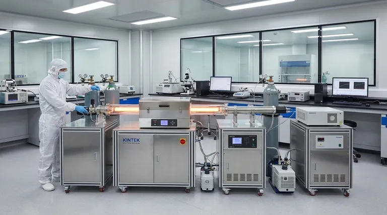
Visual Guide

Related Products
- RF PECVD System Radio Frequency Plasma Enhanced Chemical Vapor Deposition
- Slide PECVD Tube Furnace with Liquid Gasifier PECVD Machine
- Inclined Rotary Plasma Enhanced Chemical Deposition PECVD Tube Furnace Machine
- Inclined Rotary Plasma Enhanced Chemical Deposition PECVD Tube Furnace Machine
- Cylindrical Resonator MPCVD Machine System for Lab Diamond Growth
People Also Ask
- What are the advantages of PECVD in film deposition? Achieve Low-Temp, High-Quality Coatings
- What are the key advantages of PECVD technology? Achieve Low-Temperature, High-Quality Thin Film Deposition
- How is silicon dioxide deposited from tetraethylorthosilicate (TEOS) in PECVD? Achieve Low-Temperature, High-Quality SiO2 Films
- What are some promising applications of PECVD-prepared 2D materials? Unlock Advanced Sensing and Optoelectronics
- What is the role of RF power in PECVD and how does the RF-PECVD process work? Master Thin Film Deposition Control


