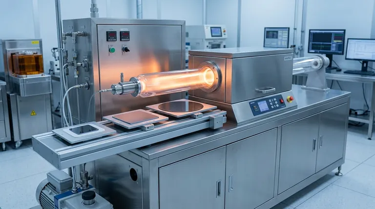
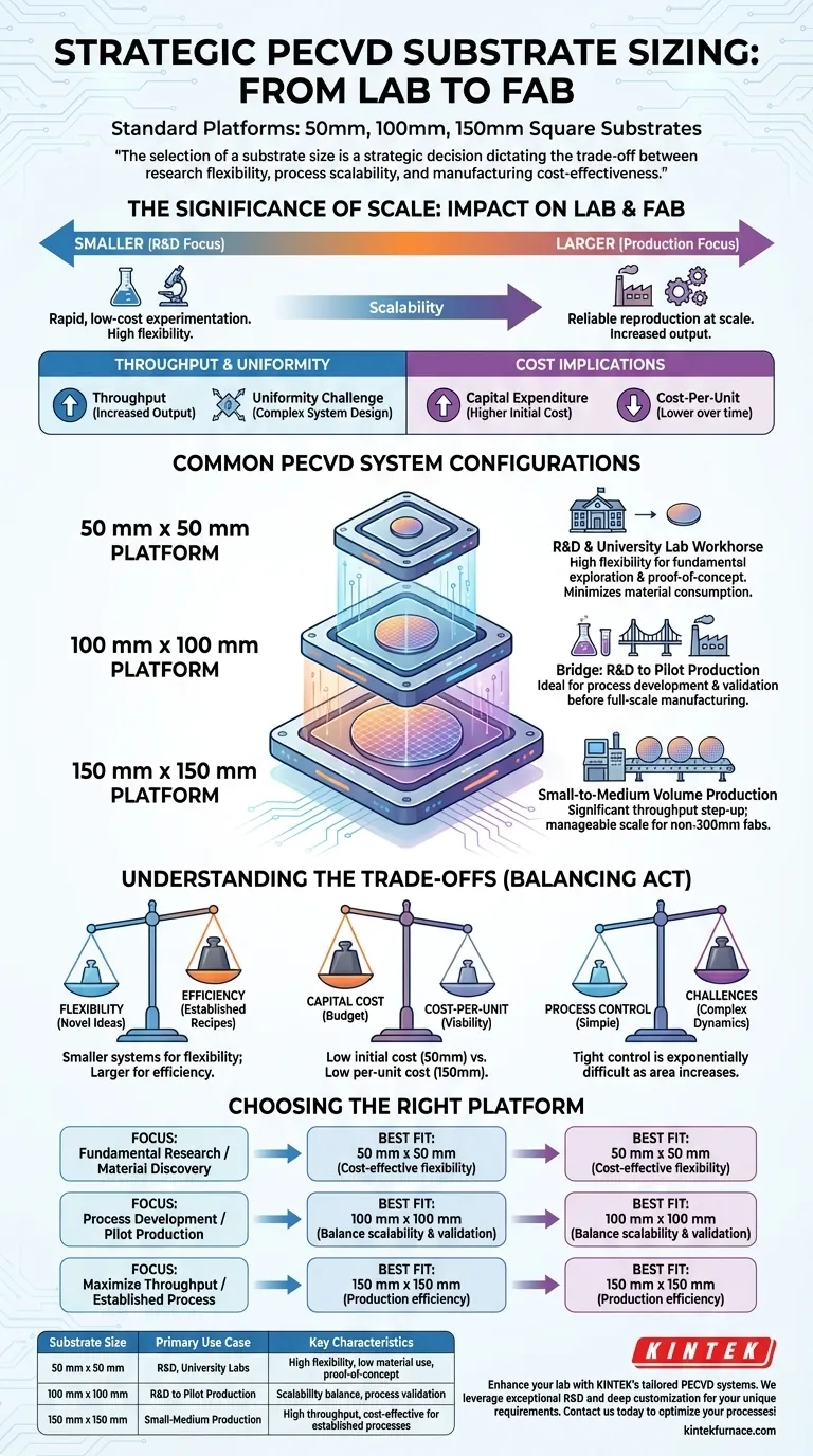
In practice, standard Plasma-Enhanced Chemical Vapor Deposition (PECVD) system platforms are most commonly configured to support square substrate sizes of 50 mm x 50 mm, 100 mm x 100 mm, and 150 mm x 150 mm. While other dimensions exist for specialized applications, these three sizes represent the industry-standard tiers for research, development, and production.
The selection of a substrate size is not merely a question of physical fit. It is a strategic decision that fundamentally dictates the trade-off between research flexibility, process scalability, and manufacturing cost-effectiveness.
The Significance of Substrate Size
Choosing a PECVD system involves more than just matching its deposition capabilities—like creating amorphous silicon or silicon nitride films—to your material needs. The physical size of the substrate holder defines the system's core purpose and economic viability.
From Lab to Fab: The Role of Scale
Smaller substrate sizes are synonymous with research and development (R&D). They allow for rapid, low-cost experimentation with new materials and processes.
As you move to larger substrates, the focus shifts from discovery to scalability and production. The goal becomes reliably reproducing a defined process on a larger scale to increase output.
Impact on Throughput and Uniformity
A larger substrate directly increases throughput, as more devices or a larger active area can be processed in a single run.
However, this comes with a significant engineering challenge: maintaining film uniformity. Ensuring consistent thickness, composition, and electrical properties across a larger surface is more complex and requires a more sophisticated system design.
Cost and Economic Implications
The capital expenditure for a larger PECVD system is significantly higher. The chamber, vacuum systems, and gas delivery modules are all more substantial.
Conversely, for high-volume manufacturing, a larger substrate reduces the cost-per-unit. The higher initial investment is offset by greater production efficiency over time.
Common PECVD System Configurations
Each standard size corresponds to a typical use case in the semiconductor, MEMS, and photonics industries.
The 50 mm x 50 mm Platform
This is the classic R&D and university lab workhorse. Its smaller size minimizes material consumption and allows for quick process iterations.
It provides maximum flexibility for scientists and engineers focused on fundamental material exploration and proof-of-concept work.
The 100 mm x 100 mm Platform
This size serves as a crucial bridge between R&D and pilot production.
It is ideal for process development teams who need to validate a process from a smaller research tool before committing to full-scale manufacturing.
The 150 mm x 150 mm Platform
This platform is geared toward small-to-medium volume production.
It offers a significant step up in throughput while still being manageable for facilities that do not require the massive scale of 300 mm wafer fabs.
Understanding the Trade-offs
The choice of platform is a balancing act. Understanding the inherent compromises is critical for making an informed decision.
Flexibility vs. Efficiency
Smaller systems offer superior flexibility for testing novel ideas. Larger systems deliver superior efficiency for executing established recipes at scale.
Capital Cost vs. Cost-Per-Unit
A low initial capital cost for a 50 mm system is attractive for research budgets. A low cost-per-unit on a 150 mm system is essential for commercial viability.
Process Control Challenges
Achieving tight process control is simplest on a small, uniform substrate. As the area increases, managing gas flow dynamics, plasma density, and temperature distribution becomes exponentially more difficult.
Choosing the Right Platform for Your Application
To make the right choice, you must align the system's capabilities with your primary objective.
- If your primary focus is fundamental research or material discovery: The 50 mm x 50 mm platform offers the most cost-effective flexibility.
- If your primary focus is process development or pilot production: The 100 mm x 100 mm platform provides the ideal balance for scaling a proven concept.
- If your primary focus is maximizing throughput for an established process: The 150 mm x 150 mm platform is designed for production environments where efficiency is key.
Ultimately, selecting the correct substrate size ensures your equipment is a strategic asset, perfectly matched to your technical and business goals.
Summary Table:
| Substrate Size | Primary Use Case | Key Characteristics |
|---|---|---|
| 50 mm x 50 mm | R&D and University Labs | High flexibility, low material consumption, ideal for proof-of-concept |
| 100 mm x 100 mm | R&D to Pilot Production | Balances scalability and process validation for development |
| 150 mm x 150 mm | Small-to-Medium Volume Production | High throughput, cost-effective for established processes |
Ready to enhance your lab's capabilities with a tailored PECVD system? At KINTEK, we leverage exceptional R&D and in-house manufacturing to provide advanced high-temperature furnace solutions, including CVD/PECVD Systems. Our strong deep customization capability ensures we precisely meet your unique experimental requirements, whether you're in research, development, or production. Contact us today to discuss how we can optimize your processes and boost efficiency!
Visual Guide
Related Products
- RF PECVD System Radio Frequency Plasma Enhanced Chemical Vapor Deposition
- Slide PECVD Tube Furnace with Liquid Gasifier PECVD Machine
- Inclined Rotary Plasma Enhanced Chemical Deposition PECVD Tube Furnace Machine
- Inclined Rotary Plasma Enhanced Chemical Deposition PECVD Tube Furnace Machine
- Cylindrical Resonator MPCVD Machine System for Lab Diamond Growth
People Also Ask
- What is RF in PECVD? A Critical Control for Plasma Deposition
- What are the applications of plasma enhanced chemical vapor deposition? Key Uses in Electronics, Optics & Materials
- How does film quality compare between PECVD and CVD? Choose the Best Method for Your Substrate
- How is silicon dioxide deposited from tetraethylorthosilicate (TEOS) in PECVD? Achieve Low-Temperature, High-Quality SiO2 Films
- What is PECVD specification? A Guide to Choosing the Right System for Your Lab


