In nanotechnology, Chemical Vapor Deposition (CVD) is a foundational fabrication method. It is the primary technique used to synthesize and grow high-purity, high-performance solid nanomaterials from gaseous precursors. Specifically, CVD is essential for creating materials like carbon nanotubes, graphene, nanowires, and other thin films with atomic-level precision.
The true significance of CVD in nanotechnology is not just its ability to create nanomaterials, but its power to control their structure with extreme precision. This control over factors like thickness, crystal structure, and morphology is what allows scientists to deliberately engineer materials with specific, predictable properties.
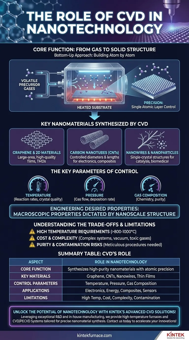
The Core Function: From Gas to Solid Structure
Chemical Vapor Deposition is a process where a substrate is exposed to one or more volatile precursor gases, which react or decompose on the substrate surface to produce the desired solid material deposit. In nanotechnology, this bottom-up approach is what enables the construction of materials atom by atom.
Building with Atomic Precision
The defining feature of CVD is its precision. By carefully managing process conditions, it is possible to control the thickness of a deposited film down to a single atomic layer.
This level of control is fundamental for creating two-dimensional (2D) materials like graphene, which is a sheet of carbon just one atom thick.
Engineering Desired Properties
A material's nanoscale structure dictates its macroscopic properties, such as electrical conductivity, strength, and optical behavior.
Because CVD allows for the synthesis of nanomaterials with a controllable morphology and size, researchers can directly engineer these properties for specific applications, moving from discovery to deliberate design.
The Key Parameters of Control
The precision of CVD stems from the ability to finely tune several key process variables:
- Temperature: Dictates the reaction rates and the crystal quality of the final material.
- Pressure: Influences the flow of gas and the deposition rate.
- Gas Composition: The choice and concentration of precursor gases determine the final material's chemistry and purity.
Key Nanomaterials Synthesized by CVD
CVD is the go-to method for a class of nanomaterials that have revolutionized multiple fields. Its versatility allows for the creation of structures that are impossible to produce with traditional top-down manufacturing.
Graphene and Other 2D Materials
CVD is the most common method for producing large-area, high-quality graphene films. It is also used to grow other novel 2D materials, such as transition metal dichalcogenides (TMDs), which have unique optoelectronic properties.
Carbon Nanotubes (CNTs)
These are cylindrical molecules of rolled-up graphene sheets. CVD enables the growth of CNTs with controlled diameters and lengths, which is critical for their application in advanced composites, electronics, and sensors.
Nanowires and Nanoparticles
CVD processes are used to synthesize single-crystal nanowires and nanoparticles. These materials are crucial for applications in electronics, catalysis, and biomedical fields due to their high surface-area-to-volume ratio.
Understanding the Trade-offs and Limitations
While powerful, CVD is not a universal solution. Understanding its limitations is crucial for making informed technical decisions.
High Temperature Requirements
Many CVD processes require extremely high temperatures, often exceeding 800-1000°C. This can limit the types of substrates that can be used and adds significantly to the energy cost of the process.
Cost and Complexity
CVD systems, especially those for high-purity research or large-scale production, can be complex and expensive to acquire, operate, and maintain. The process often involves vacuum systems and the handling of toxic or flammable gases.
Purity and Contamination Risks
The final material's quality is highly sensitive to impurities in the precursor gases or the reaction chamber. Preventing contamination requires meticulous procedures and high-purity source materials, which adds to the overall cost and complexity.
Making the Right Choice for Your Goal
Your specific objective determines how you should leverage CVD technology. The process is not a single tool but a versatile platform for achieving distinct outcomes in nanoscience and engineering.
- If your primary focus is foundational research: CVD offers unparalleled control for creating novel materials with specifically engineered crystal structures and properties for testing new scientific theories.
- If your primary focus is next-generation electronics: CVD is the established, scalable method for producing the high-quality graphene and thin films required for advanced transistors, sensors, and optoelectronic devices.
- If your primary focus is advanced materials and energy: Use CVD to synthesize high-surface-area nanomaterials like carbon nanotubes and nanowires for applications in energy storage, catalysis, and high-strength composites.
Ultimately, mastering CVD is essential for anyone aiming to move from the concept of a nanomaterial to its real-world application.
Summary Table:
| Aspect | Role in Nanotechnology |
|---|---|
| Core Function | Synthesizes high-purity nanomaterials from gaseous precursors with atomic precision |
| Key Materials | Graphene, carbon nanotubes, nanowires, thin films |
| Control Parameters | Temperature, pressure, gas composition |
| Applications | Electronics, energy storage, composites, sensors |
| Limitations | High temperature requirements, cost, complexity, contamination risks |
Unlock the potential of nanotechnology with KINTEK's advanced CVD solutions! Leveraging exceptional R&D and in-house manufacturing, we provide high-temperature furnaces, including CVD/PECVD Systems, tailored for precise nanomaterial synthesis. Whether you're in research, electronics, or materials science, our deep customization capabilities ensure your unique experimental needs are met. Contact us today to discuss how our expertise can accelerate your innovations!
Visual Guide
Related Products
- Custom Made Versatile CVD Tube Furnace Chemical Vapor Deposition CVD Equipment Machine
- Multi Heating Zones CVD Tube Furnace Machine for Chemical Vapor Deposition Equipment
- HFCVD Machine System Equipment for Drawing Die Nano Diamond Coating
- Split Chamber CVD Tube Furnace with Vacuum Station CVD Machine
- 915MHz MPCVD Diamond Machine Microwave Plasma Chemical Vapor Deposition System Reactor
People Also Ask
- What is a CVD tube furnace and what is its primary function? Discover Precision Thin-Film Deposition
- What customization options are available for CVD tube furnaces? Tailor Your System for Superior Material Synthesis
- What are the key application fields of CVD tube furnaces? Unlock Precision in Thin-Film Synthesis
- What future trends are expected in the development of CVD tube furnaces? Discover Smarter, More Versatile Systems
- What temperature range do standard CVD tube furnaces operate at? Unlock Precision for Your Material Deposition