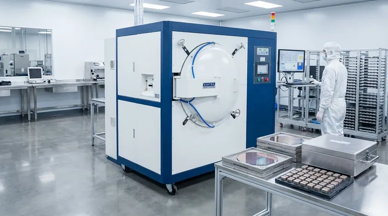
In modern electronics manufacturing, vacuum furnaces are critical tools used for highly controlled thermal processes. They are essential for creating special performance materials, processing semiconductor wafers, and sintering complex components like multi-layer ceramic capacitors (MLCCs) and integrated circuits.
The fundamental role of a vacuum furnace is not just to heat materials, but to do so in an ultra-clean environment. By removing air and other reactive gases, these furnaces prevent contamination and unwanted chemical reactions that would otherwise degrade the performance and reliability of sensitive electronic components.
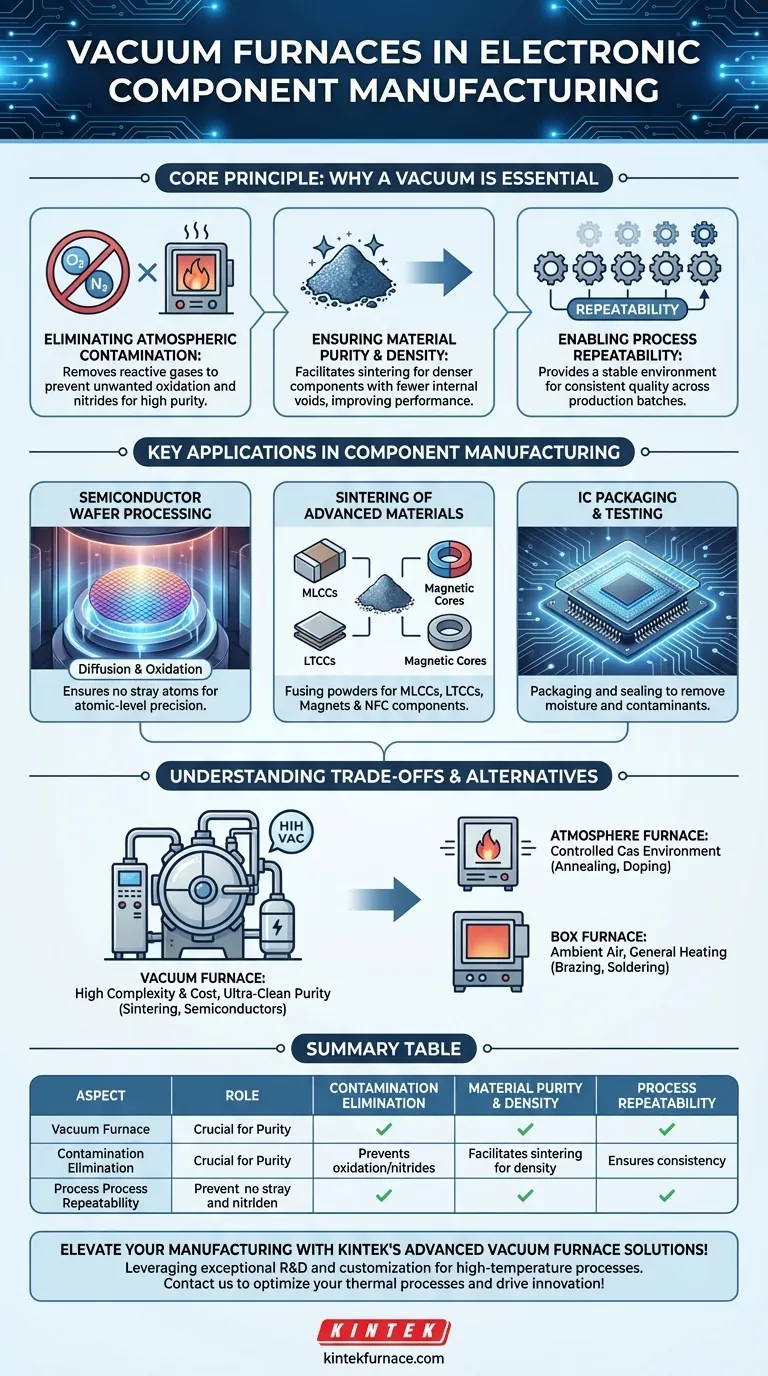
The Core Principle: Why a Vacuum is Essential
The primary advantage of a vacuum furnace is its ability to precisely control the processing atmosphere. This control is fundamental to achieving the purity and structural integrity required in high-performance electronics.
Eliminating Atmospheric Contamination
At the high temperatures required for manufacturing, materials can easily react with gases present in the air, primarily oxygen and nitrogen. A vacuum removes these reactive elements, creating a near-perfectly clean environment.
This prevents the formation of unintended oxides or nitrides on the material's surface, which can drastically alter its electrical properties.
Ensuring Material Purity and Density
Processes like sintering involve fusing powdered materials together under heat to form a solid object. In a vacuum, trapped gases are pulled out from between the powder particles.
This allows for the creation of denser, stronger components with fewer internal voids, leading to superior mechanical and electrical performance in parts like ceramic cores and magnetic materials.
Enabling Process Repeatability
By removing the variable of atmospheric composition, vacuum furnaces provide an exceptionally stable and repeatable processing environment. Each production batch can be subjected to the exact same conditions, ensuring consistent quality and performance across millions of components.
Key Applications in Component Manufacturing
Vacuum furnaces are not used for all heating processes, but they are indispensable for the most sensitive and demanding steps where material integrity is paramount.
Semiconductor Wafer Processing
The creation of microchips involves depositing and modifying materials at an atomic level. Vacuum furnaces are used for critical steps like diffusion (introducing dopants into the silicon wafer) and oxidation (growing a pure, thin layer of silicon dioxide).
Performing these tasks in a vacuum ensures that no stray atoms from the air are incorporated into the semiconductor, which would create fatal defects.
Sintering of Advanced Materials
Many vital electronic components are made from ceramic or metallic powders. Vacuum sintering furnaces are used for the debinding, pre-sintering, and final sintering of materials for:
- Multi-Layer Ceramic Capacitors (MLCCs)
- Low-Temperature Co-fired Ceramics (LTCCs)
- Magnetic Materials and NFC components
This process creates the dense, final form of the component while protecting its delicate material composition.
Integrated Circuit (IC) Packaging and Testing
After a chip is fabricated, it must be packaged to protect it and connect it to the outside world. Certain packaging and sealing steps are performed in a vacuum to remove any moisture or contaminants that could cause corrosion or failure later in the product's life.
Understanding the Trade-offs and Alternatives
While powerful, a vacuum furnace is not always the right or only tool for thermal processing in electronics. Understanding the alternatives clarifies its specific role.
The Cost and Complexity of Vacuum
Vacuum furnaces are significantly more complex and expensive than their atmospheric counterparts. They require robust vacuum pumps, precise seals, and longer process cycles to pump down the chamber, making them less efficient for simple heating tasks.
When an Atmosphere Furnace Is Used
Sometimes, a process requires a specific gas, not the absence of one. Atmosphere furnaces are used to create a controlled environment of inert gases (like argon or nitrogen) or reactive gases for processes like controlled doping or annealing of semiconductor materials.
The Role of Simpler Box Furnaces
For many general-purpose applications, a simple box furnace that operates in ambient air is sufficient. Processes like brazing (joining metals), reflow soldering, and basic heat treatment to enhance durability often do not require the purity of a vacuum environment and can be done more cost-effectively without it.
Making the Right Choice for Your Goal
Selecting the correct thermal processing technology depends entirely on the material requirements and the desired outcome for the component.
- If your primary focus is material purity and atomic-level precision: A vacuum furnace is non-negotiable for tasks like semiconductor diffusion and growing pure oxide layers.
- If your primary focus is creating dense, high-performance parts from powders: Vacuum sintering is the industry standard for producing reliable MLCCs, magnets, and advanced ceramics.
- If your primary focus is mechanical joining or general heat treatment: A simpler and more cost-effective box or atmosphere furnace is often the more practical choice for processes like brazing and soldering.
Ultimately, mastering the thermal environment is fundamental to the successful manufacturing of high-performance electronic components.
Summary Table:
| Aspect | Role in Electronics Manufacturing |
|---|---|
| Contamination Elimination | Removes reactive gases to prevent oxidation and nitrides, ensuring high material purity. |
| Material Purity and Density | Facilitates sintering for denser components with fewer voids, improving electrical performance. |
| Process Repeatability | Provides stable vacuum environment for consistent quality across production batches. |
| Key Applications | Used in semiconductor wafer processing, sintering MLCCs, and IC packaging for reliability. |
Elevate your electronic component manufacturing with KINTEK's advanced vacuum furnace solutions! Leveraging exceptional R&D and in-house manufacturing, we provide high-temperature furnaces like Muffle, Tube, Rotary, Vacuum & Atmosphere Furnaces, and CVD/PECVD Systems. Our deep customization capabilities ensure precise alignment with your unique experimental needs, enhancing purity, efficiency, and reliability. Contact us today to discuss how our tailored solutions can optimize your thermal processes and drive innovation in your lab!
Visual Guide
Related Products
- Vacuum Hot Press Furnace Machine Heated Vacuum Press Tube Furnace
- Vacuum Hot Press Furnace Machine Heated Vacuum Press
- 600T Vacuum Induction Hot Press Vacuum Heat Treat and Sintering Furnace
- 2200 ℃ Tungsten Vacuum Heat Treat and Sintering Furnace
- Vacuum Heat Treat Sintering Furnace with Pressure for Vacuum Sintering
People Also Ask
- Why use Vacuum Hot Press (VHP) for ZnS Ceramics? Achieve Superior IR Transparency and Mechanical Strength
- Which process parameters must be optimized for specific materials in a vacuum hot press furnace? Achieve Optimal Density and Microstructure
- What are the benefits of the vacuum environment system in a vacuum hot press furnace? Unlock High-Density Sintering
- Why is a high vacuum environment crucial when preparing copper-carbon nanotube composites in a vacuum hot press furnace? Achieve Superior Composite Integrity
- How does a vacuum hot press furnace promote densification in the manufacturing of graphite flake/copper composites? Achieve Superior Composite Materials


