At its core, a Microwave Plasma Chemical Vapor Deposition (MPCVD) system is a highly specialized machine designed to grow synthetic diamonds and other advanced carbon materials. It uses microwave energy to create a plasma from specific gases, allowing carbon atoms to settle onto a substrate and arrange themselves into a perfect crystalline structure, building a high-purity film atom by atom.
The central purpose of an MPCVD system is not just to make materials, but to engineer them at a fundamental level. It provides the necessary control over temperature, pressure, and purity to create exceptionally high-performance materials like diamond, which are impossible to produce with conventional methods.
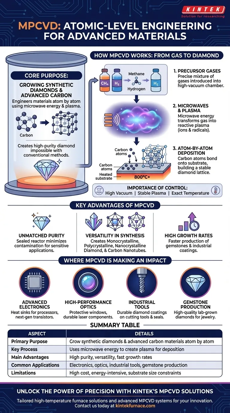
How MPCVD Works: From Gas to Diamond
An MPCVD system functions like a high-tech atomic construction chamber, meticulously assembling materials from a gaseous state.
The Core Principle: Precursor Gases
The process begins by introducing a precise mixture of gases, known as precursors, into a high-vacuum chamber. For diamond growth, this is typically a combination of a carbon source (like methane) and hydrogen.
The Role of Microwaves
This gas mixture is then energized with powerful microwaves. This energy strips electrons from the gas molecules, transforming them into a plasma—a highly reactive cloud of ions and radicals that glows brightly.
Atom-by-Atom Deposition
Within this plasma, carbon atoms are deposited onto a prepared substrate. The carefully controlled conditions—including high temperatures often exceeding 800°C—encourage these atoms to bond together in the strong, stable diamond crystal lattice.
The Importance of Control
The quality of the final product depends entirely on precision. The system's ability to maintain a high vacuum, a stable plasma, and exact temperatures is what determines whether the result is a flawless single-crystal diamond or a less-ordered polycrystalline film.
Key Advantages of the MPCVD Process
The complexity of the system is justified by the unique capabilities it offers, particularly in creating materials with superior properties.
Unmatched Purity and Quality
The process takes place in a sealed, metal reactor under a high vacuum. This design minimizes contamination from the atmosphere or the chamber itself, resulting in diamond films of exceptional purity, which is critical for sensitive electronic and optical applications.
Versatility in Material Synthesis
MPCVD is not limited to one type of material. By adjusting the process parameters, operators can create a range of structures, including:
- Monocrystalline Diamond: Single, flawless crystals for high-end electronics and gems.
- Polycrystalline Diamond: Conglomerates of smaller crystals, ideal for durable coatings on cutting tools and wear-resistant parts.
- Nanocrystalline Diamond: Extremely small crystals forming a super-smooth, low-friction surface.
- Carbon Nanotubes and Nanowires: Advanced materials for next-generation research.
High Growth Rates
Compared to other deposition methods, the stable plasma and wide operating pressure range of an MPCVD system can enable a faster growth rate, making it more commercially viable for producing materials like lab-grown gemstones and industrial diamond coatings.
Understanding the Trade-offs
While powerful, MPCVD technology is not without its practical limitations. It is a specialized tool for demanding applications.
System Complexity and Cost
These are sophisticated, high-vacuum systems that represent a significant capital investment. They require specialized training to operate and maintain, unlike simpler manufacturing equipment.
High Energy Consumption
Generating and sustaining a stable, high-temperature plasma is an energy-intensive process. This contributes to the operational cost and is a key consideration for large-scale production.
Substrate and Size Limitations
Deposition occurs within a finite chamber and is limited to the surface area of the substrate. This inherently restricts the overall size and shape of the objects that can be created or coated directly.
Where MPCVD is Making an Impact
The ability to engineer diamond has unlocked new possibilities across several high-tech industries.
Advanced Electronics and Semiconductors
Diamond is an exceptional thermal conductor and a wide-bandgap semiconductor. MPCVD allows for its use as a heat sink for high-power processors and in creating next-generation transistors that can operate at higher frequencies and temperatures.
High-Performance Optics
Diamond's extreme hardness and optical transparency make it an ideal material for protective windows, durable lenses for harsh environments, and components for high-power lasers.
Industrial Tools and Wearable Parts
Coating cutting tools, drill bits, or mechanical seals with a layer of polycrystalline diamond dramatically increases their lifespan and performance.
Gemstone Production
MPCVD is a leading method for producing high-quality, lab-grown diamonds for the jewelry industry that are chemically and physically identical to their mined counterparts.
Making the Right Choice for Your Goal
To apply this technology effectively, you must align its capabilities with your primary objective.
- If your primary focus is industrial manufacturing (e.g., cutting tools, heat sinks): MPCVD's ability to deposit durable, polycrystalline diamond films at relatively high growth rates is the key benefit.
- If your primary focus is high-end electronics or optics: The system's precision in growing ultra-pure, monocrystalline diamond films is its most critical feature.
- If your primary focus is fundamental materials research: The versatility to create different diamond forms, carbon nanotubes, and nanowires makes it an indispensable tool for exploration.
Ultimately, MPCVD provides an atomic-level construction method for creating materials that were once considered impossible to engineer.

Summary Table:
| Aspect | Details |
|---|---|
| Primary Purpose | Grow synthetic diamonds and advanced carbon materials atom by atom |
| Key Process | Uses microwave energy to create plasma from gases for deposition |
| Main Advantages | High purity, versatility in material types, fast growth rates |
| Common Applications | Electronics, optics, industrial tools, gemstone production |
| Limitations | High cost, energy-intensive, substrate size constraints |
Unlock the Power of Precision with KINTEK's MPCVD Solutions
Are you advancing electronics, optics, or industrial applications with high-purity diamond films? KINTEK leverages exceptional R&D and in-house manufacturing to provide tailored high-temperature furnace solutions, including advanced MPCVD systems. Our expertise in deep customization ensures we meet your unique experimental needs, whether for monocrystalline diamond growth or versatile carbon material synthesis.
Contact us today to discuss how our MPCVD systems can drive your innovation forward!
Visual Guide
Related Products
- 915MHz MPCVD Diamond Machine Microwave Plasma Chemical Vapor Deposition System Reactor
- MPCVD Machine System Reactor Bell-jar Resonator for Lab and Diamond Growth
- Cylindrical Resonator MPCVD Machine System for Lab Diamond Growth
- RF PECVD System Radio Frequency Plasma Enhanced Chemical Vapor Deposition
- Slide PECVD Tube Furnace with Liquid Gasifier PECVD Machine
People Also Ask
- What are some key features and benefits of the microwave plasma chemical vapor deposition system? Achieve Unmatched Material Synthesis
- In which industries is the microwave plasma chemical vapor deposition system commonly used? Unlock High-Purity Material Synthesis
- What are the essential components of an MPCVD reactor system? Build a Pristine Environment for High-Purity Materials
- How does the MPCVD process work to deposit diamond? A Guide to High-Purity Synthesis
- What is the basic principle of operation for the microwave plasma chemical vapor deposition system? Unlock High-Purity Material Growth


