At its core, the significance of Chemical Vapor Deposition (CVD) in industrial applications is its unique ability to engineer material surfaces at the atomic level. This process allows for the creation of ultra-thin, exceptionally pure, and highly uniform films that bestow entirely new properties—such as electrical conductivity, extreme hardness, or biocompatibility—onto a base material, making it a cornerstone technology for modern manufacturing.
Chemical Vapor Deposition is not merely a coating technique; it is a fundamental enabling process. It empowers industries to move beyond the limitations of bulk materials and design surfaces with precisely the properties needed to unlock next-generation performance in electronics, energy, aerospace, and medicine.
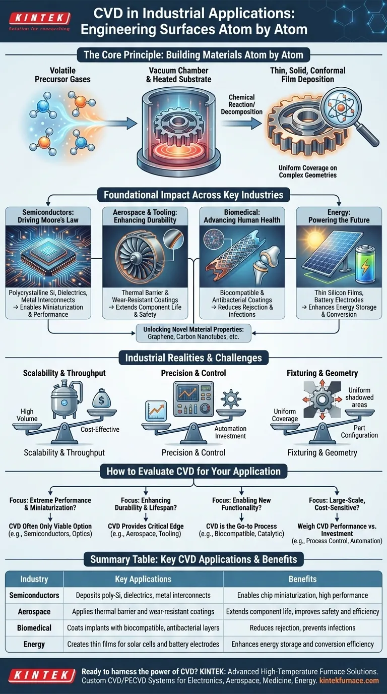
The Core Principle: Building Materials Atom by Atom
CVD is a process where a substrate (the part to be coated) is placed in a vacuum chamber and exposed to one or more volatile precursor gases. When these gases interact on or near the heated substrate surface, they react or decompose, depositing a thin, solid film onto the material.
The Power of Conformal Coatings
A key advantage of CVD is its ability to produce conformal films. Because the coating is built from a gas phase, it can uniformly cover highly complex, non-line-of-sight surfaces and intricate 3D geometries.
This is something that traditional line-of-sight techniques, like spraying or physical vapor deposition (PVD), simply cannot achieve with the same level of precision.
Unlocking Novel Material Properties
CVD is not limited to depositing existing materials. It is a primary method for creating advanced materials with unique electrical, thermal, and mechanical properties that are difficult or impossible to form otherwise.
This includes synthesizing materials like graphene, carbon nanotubes, and specific dielectric layers, which are foundational to many advanced technologies.
Foundational Impact Across Key Industries
The versatility of CVD means its impact is felt across nearly every high-technology sector. It is often the unseen innovation that makes a final product possible.
Driving Moore's Law in Semiconductors
The semiconductor industry is arguably the largest user of CVD. It is essential for manufacturing integrated circuits.
CVD is used to deposit the polycrystalline silicon for transistor gates, the dielectric layers that provide electrical isolation between components, and the metal interconnects (like tungsten and copper) that wire the chip together. Without it, modern chip miniaturization would be impossible.
Enhancing Durability in Aerospace and Tooling
In aerospace, engine components like turbine blades are exposed to extreme temperatures and corrosive environments. CVD is used to apply thermal barrier and wear-resistant coatings.
These coatings significantly extend component life, improve fuel efficiency, and enhance safety in demanding operational conditions.
Advancing Human Health in the Biomedical Field
CVD plays a critical role in making medical devices safer and more effective. It is used to apply ultra-thin, biocompatible coatings to implants like stents and artificial joints, preventing rejection by the body.
Additionally, it can create antibacterial surfaces on medical tools, reducing the risk of hospital-acquired infections.
Powering the Future of Energy
In the renewable energy sector, CVD is used to create the thin silicon films that form the basis of many photovoltaic solar cells.
It is also a key process for developing advanced battery electrodes and membranes, contributing directly to more efficient energy storage and conversion.
Understanding the Trade-offs and Industrial Realities
While powerful, successfully implementing CVD at an industrial scale requires navigating several key challenges. It is not a simple "plug-and-play" solution.
The Challenge of Scalability and Throughput
A process that works perfectly in a research lab may not be viable for mass production. A major industrial consideration is achieving high throughput to make the process cost-effective.
This involves designing large-batch reactors and optimizing process times without sacrificing coating quality or uniformity.
The Need for Precision and Control
The performance of a CVD coating is extremely sensitive to process variables like temperature, pressure, and gas flow rates. Advanced process control and automation are essential for ensuring consistency and repeatability.
For high-value applications like semiconductors, this precision is non-negotiable and represents a significant engineering investment.
Fixturing and Part Geometry
The way a part is held (fixturing) inside the coating chamber is critical. Poor fixturing can create "shadowed" areas where the gas cannot reach, leading to an incomplete or non-uniform coating.
The complexity of the part's configuration must be accounted for to ensure the conformal coating is applied everywhere it is needed.
How to Evaluate CVD for Your Application
Choosing the right surface enhancement technology depends entirely on your end goal. CVD is a high-performance solution for challenges that cannot be met by simpler methods.
- If your primary focus is extreme performance and miniaturization: CVD is often the only viable option, especially for applications in semiconductors and advanced optics where atomic-level precision is required.
- If your primary focus is enhancing durability and lifespan: CVD provides a critical performance edge for tools and components in aerospace or heavy industry, justifying its cost through extended operational life.
- If your primary focus is enabling new functionality: CVD is the go-to process for creating surfaces with novel capabilities, such as biocompatibility for medical implants or catalytic activity for chemical processing.
- If your primary focus is large-scale, cost-sensitive production: You must heavily weigh the need for CVD's performance against the significant investment in process control, automation, and throughput optimization.
Ultimately, Chemical Vapor Deposition empowers engineers to design material properties on demand, transforming passive surfaces into active, high-performance components.
Summary Table:
| Industry | Key CVD Applications | Benefits |
|---|---|---|
| Semiconductors | Deposits poly-Si, dielectrics, metal interconnects | Enables chip miniaturization, high performance |
| Aerospace | Applies thermal barrier and wear-resistant coatings | Extends component life, improves safety and efficiency |
| Biomedical | Coats implants with biocompatible, antibacterial layers | Reduces rejection, prevents infections |
| Energy | Creates thin films for solar cells and battery electrodes | Enhances energy storage and conversion efficiency |
Ready to harness the power of CVD for your industrial challenges? At KINTEK, we leverage exceptional R&D and in-house manufacturing to provide advanced high-temperature furnace solutions, including CVD/PECVD Systems. Our strong deep customization capability ensures we precisely meet your unique experimental requirements, whether you're in electronics, aerospace, medicine, or energy. Contact us today to discuss how our tailored solutions can drive your innovation forward!
Visual Guide
Related Products
- Custom Made Versatile CVD Tube Furnace Chemical Vapor Deposition CVD Equipment Machine
- Multi Heating Zones CVD Tube Furnace Machine for Chemical Vapor Deposition Equipment
- HFCVD Machine System Equipment for Drawing Die Nano Diamond Coating
- Split Chamber CVD Tube Furnace with Vacuum Station CVD Machine
- 915MHz MPCVD Diamond Machine Microwave Plasma Chemical Vapor Deposition System Reactor
People Also Ask
- What temperature range do standard CVD tube furnaces operate at? Unlock Precision for Your Material Deposition
- How can integrating CVD tube furnaces with other technologies benefit device fabrication? Unlock Advanced Hybrid Processes
- What are the practical applications of gate media prepared by CVD tube furnaces? Unlock Advanced Electronics and More
- Which industries and research fields benefit from CVD tube furnace sintering systems for 2D materials? Unlock Next-Gen Tech Innovations
- How does CVD tube furnace sintering enhance graphene growth? Achieve Superior Crystallinity and High Electron Mobility