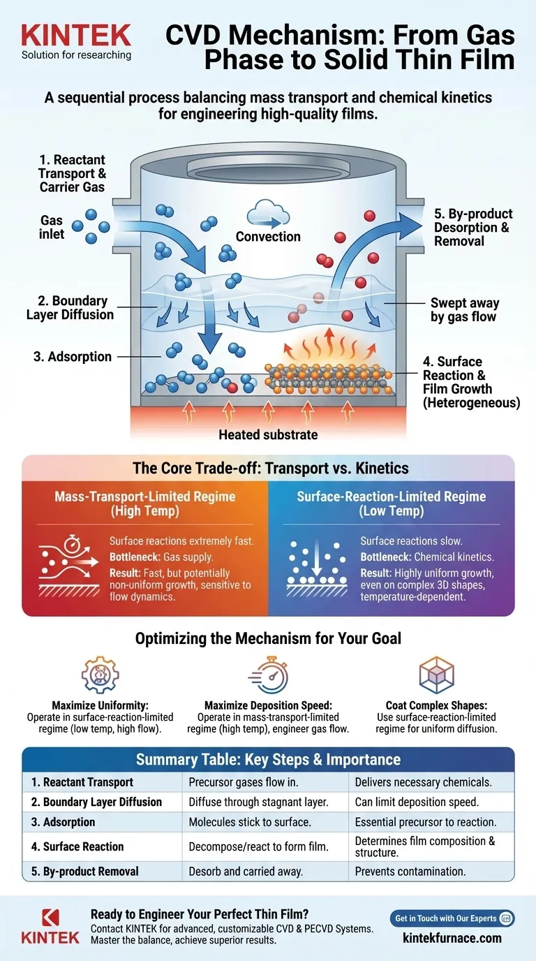
The mechanism of a Chemical Vapor Deposition (CVD) reaction is a sequential process where volatile chemical precursors in a gas phase react to form a solid film on a heated substrate. This involves transporting the reactive gases to the substrate, a series of chemical reactions on or near the surface, the subsequent formation of the film, and the removal of gaseous by-products from the reaction chamber.
At its core, the CVD mechanism is a competition between two fundamental rates: the rate at which precursor gases are supplied to the substrate (mass transport) and the rate at which they chemically react on the surface (kinetics). Understanding and controlling this balance is the key to engineering high-quality, uniform thin films.
Deconstructing the CVD Process: From Gas to Solid Film
To truly understand the CVD mechanism, we must break it down into its distinct physical and chemical steps. Each step presents an opportunity for control and a potential bottleneck for the overall process.
Step 1: Transport of Reactants into the Chamber
The process begins by introducing one or more volatile precursor gases into the reaction chamber.
A carrier gas (often an inert gas like argon or nitrogen) is typically used to dilute the precursors and transport them toward the substrate via convection. Flow rates must be precisely controlled to maintain the desired chemical concentrations.
Step 2: Diffusion Through the Boundary Layer
As the gas flows over the heated substrate, a stagnant "boundary layer" of gas forms just above the surface.
Reactant species must diffuse through this layer to reach the substrate. The thickness of this layer and the speed of diffusion are critical factors that can limit the overall deposition rate.
Step 3: Adsorption onto the Substrate
Once a precursor molecule reaches the substrate, it must physically stick to the surface, a process known as adsorption.
The molecule does not immediately react. It may diffuse across the surface, moving around until it finds an energetically favorable site to bond and react.
Step 4: The Surface Reaction and Film Growth
This is the heart of the CVD process. Through thermal energy from the heated substrate, the adsorbed precursor molecules decompose and/or react with each other.
This heterogeneous surface reaction breaks chemical bonds, leaving behind the desired solid material, which nucleates and grows into a continuous thin film. The specific chemical pathway determines the film's composition and microstructure.
Step 5: Desorption and Removal of By-products
The chemical reactions that form the solid film also produce volatile by-products.
These by-product molecules must desorb (detach) from the surface, diffuse back out through the boundary layer, and be swept away by the gas flow. Inefficient removal of by-products can contaminate the film or inhibit further growth.
Understanding the Core Trade-off: Transport vs. Kinetics
The final quality and growth rate of the film are governed by which of the preceding steps is the slowest, or "rate-limiting." This typically falls into one of two regimes.
Mass-Transport-Limited Regime
In this regime, typically at higher temperatures, the surface reactions are extremely fast. The bottleneck is the supply of fresh reactants to the surface.
The growth rate becomes highly sensitive to gas flow dynamics, chamber pressure, and the geometry of the reactor. This can lead to non-uniform coatings, as areas with more direct gas flow grow faster.
Surface-Reaction-Limited Regime
At lower temperatures, the surface reactions are much slower than the rate at which precursors arrive. The bottleneck is the chemical kinetics itself.
Because there is an ample supply of reactants everywhere on the surface, deposition tends to be highly uniform, even on complex 3D shapes. The growth rate in this regime is strongly dependent on temperature.
Optimizing the Mechanism for Your Goal
The ideal CVD process parameters depend entirely on the desired outcome for your film. By controlling temperature, pressure, and gas flow, you are directly manipulating the balance between mass transport and reaction kinetics.
- If your primary focus is film uniformity: Operate in the surface-reaction-limited regime (lower temperature, higher precursor flow) to ensure the growth rate is consistent across the entire substrate.
- If your primary focus is maximum deposition speed: Operate in the mass-transport-limited regime (higher temperature) but be prepared to engineer the gas flow to mitigate potential non-uniformity.
- If your primary focus is coating complex geometries: Use the surface-reaction-limited regime, as it ensures reactants have time to diffuse into and uniformly coat intricate features.
Mastering the CVD mechanism means moving beyond a simple recipe and learning to tune the fundamental process steps to achieve your specific material goals.
Summary Table:
| CVD Mechanism Step | Key Process | Importance |
|---|---|---|
| 1. Reactant Transport | Precursor gases flow into the chamber. | Delivers necessary chemicals to the substrate. |
| 2. Boundary Layer Diffusion | Reactants diffuse through the stagnant gas layer. | Can be a rate-limiting step for deposition speed. |
| 3. Adsorption | Molecules stick to the substrate surface. | Essential precursor to the main chemical reaction. |
| 4. Surface Reaction | Precursors decompose/react to form the solid film. | Core step determining film composition and structure. |
| 5. By-product Removal | Volatile by-products desorb and are carried away. | Prevents contamination and allows continuous growth. |
Ready to Engineer Your Perfect Thin Film?
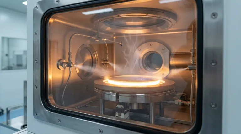
Understanding the delicate balance between gas transport and surface kinetics is key to optimizing any CVD process. At KINTEK, we leverage our exceptional R&D and in-house manufacturing to transform this understanding into results.
Whether your goal is extreme uniformity, high deposition rates, or coating complex 3D structures, our advanced CVD and PECVD Systems are engineered with the deep customization capability to precisely meet your unique experimental requirements.
Contact us today to discuss how we can help you master your CVD mechanism and achieve superior thin films.
Visual Guide
Related Products
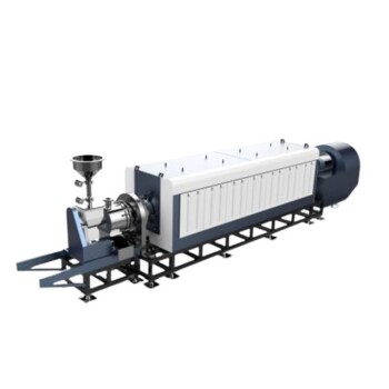
- MPCVD Machine System Reactor Bell-jar Resonator for Lab and Diamond Growth
- Custom Made Versatile CVD Tube Furnace Chemical Vapor Deposition CVD Equipment Machine
- 915MHz MPCVD Diamond Machine Microwave Plasma Chemical Vapor Deposition System Reactor
- Cylindrical Resonator MPCVD Machine System for Lab Diamond Growth
- Slide PECVD Tube Furnace with Liquid Gasifier PECVD Machine
People Also Ask
- What are the key components of an MPCVD system? Unlock High-Purity Crystal Growth
- What are the essential components of an MPCVD reactor system? Build a Pristine Environment for High-Purity Materials
- How do carbon-containing groups contribute to diamond growth in the MPCVD method? Unlock High-Quality Diamond Synthesis
- How does pressure affect the MPCVD growth process? Master Plasma Control for Superior Film Quality
- What are the advantages of MPCVD over LPCVD and PECVD? Achieve Superior Film Quality and Uniformity