The sintering of mixed-conducting oxides is transformed by an electron wind that drags ions into place.
In these materials, a high electronic current density creates a powerful, directed flux of electrons that physically couples with and pushes lattice cations—a phenomenon measured by the charge-of-transport coefficient. This coupled electron‑ion mass transport generates an additional ionic flux that can rival or even surpass the material’s natural ionic conductivity. The practical result is dramatically faster densification at significantly lower furnace temperatures, enabling precise control over the final microstructure.
In mixed ionic‑electronic conductors, the electron‑ion correlation effect converts an electrical current directly into mechanical mass transport. The core insight: by tuning the electronic flux rather than relying solely on thermal activation, you can decouple densification from the thermal budget. This unlocks rapid, low‑temperature sintering of semiconducting ceramics that are otherwise stubborn to consolidate.
The Mechanism: How Electrons Become a Delivery Vehicle for Ions
The Charge‑of‑Transport Effect is a Direct Drag Phenomenon
In a pure ionic conductor, mass transport relies on chemical potential gradients or external electric fields that act on charged ions alone. In a mixed conductor, a large electronic current introduces a completely different pathway. The moving electrons do not merely pass by the lattice; they scatter off and transfer momentum to the cations. This physical drag forces an extra ionic drift in the direction of electron flow. The strength of this coupling is captured by the charge‑of‑transport coefficient, which quantifies how many ions are effectively dragged per electron.
This Flux Often Outpaces Conventional Ionic Conductivity
Under high‑current field‑assisted processing, the flux generated by electron drag is not a minor perturbation. In materials like FeO, CoO, or TiO₂, the dragged ionic flux can equal or even exceed the flux from standard ionic conduction. The key is that the driving force is the electronic current density, not just temperature. A massive electron flow can be engineered at temperatures where normal ionic mobility is sluggish, creating an effectively amplified, low‑temperature diffusion pathway.
The Mechanism is Electrode‑Reaction Independent
Typical field‑assisted sintering techniques—like spark plasma sintering—often rely on current to modify interfacial reactions or generate plasma. In mixed conductors, the densification mechanism described here does not depend on such electrode‑limited processes. The drag acts as a bulk effect within the material, driven purely by the internal electronic flux. This means the entire compact experiences the enhanced transport, not just regions near the electrodes, leading to more homogeneous densification when current paths are controlled.
The Practical Significance: Rethinking Thermal Budgets
Densification Decouples From Furnace Temperature
Because mass transport is carried by the electron wind, you no longer need to ramp the furnace to extreme temperatures where ionic conductivity alone becomes sufficient. By pushing a high electronic current through the semiconducting compact at a lower overall thermal budget, you achieve the same level of densification much faster. This is a profound shift for processing temperature‑sensitive compositions that would otherwise suffer from grain growth, phase decomposition, or volatile element loss.
Microstructure Control Becomes a Current‑Profiling Exercise
The densification rate becomes a function of the applied current profile—current intensity, waveform, and duration. Instead of only tuning temperature‑time schedules, materials scientists can design targeted current trajectories. For example, a short burst of high current at an intermediate temperature can initiate rapid densification, then a lower‑current hold can relieve residual stresses. This opens the door to unprecedented microstructural engineering: finer grains, tailored porosity distributions, and higher final densities without coarsening.
Process Scaling is Feasible in Modern Field‑Assisted Furnaces
High‑current field‑assisted sintering furnaces are commercially available and can be instrumented to deliver programmed current profiles. The electron‑drag mechanism does not require exotic equipment; it leverages the inherent mixed conductivity of the workpiece. As long as the material exhibits sufficient electronic conductivity at the processing temperature, the effect can be activated. This makes it a practical, scalable route for manufacturing dense, high‑performance ceramic components such as solid oxide fuel cell electrolytes, oxygen transport membranes, and conducting oxides for electronics.
Understanding the Trade‑offs and Limitations
Electronic Conductivity Must Dominate
The charge‑of‑transport effect is a correlation between electrons and ions. If the material is dominated by ionic transport or is an insulator, there are too few free electrons to generate a meaningful drag. The technique applies specifically to mixed conductors with a substantial electronic contribution. Purely ionic conductors will not benefit from this mechanism, and attempts to force a current through them may cause local heating or electrical breakdown.
Current Distribution Can Create Hot Spots
High current densities generate Joule heating. If the current path is not uniformly distributed—due to sample geometry, porosity gradients, or contact resistance—localized overheating can occur. This may lead to heterogeneous densification, internal stresses, or even core‑shell microstructures. Careful electrode design, pre‑compaction homogeneity, and real‑time current monitoring are essential to avoid sacrificing uniformity.
There is a Narrow Process Window
The coupling efficiency depends on temperature, current density, and material composition. Too low a current fails to activate the drag; too high a current risks melting or decomposing the material. Finding the optimal window requires precise characterization of the charge‑of‑transport coefficient for each system. Blind application without understanding the material‑specific threshold can lead to under‑ or over‑processing. It is not a “plug‑and‑play” technique but one that rewards careful parameter mapping.
Making the Right Choice for Your Sintering Process
Selecting a field‑assisted approach based on electron‑ion correlation is not a universal recipe—it is a targeted strategy for the right material class and a well‑characterized system.
- If your primary focus is densifying a temperature‑sensitive mixed conductor: Leverage a high‑current pulse at a moderate temperature to kickstart densification while preserving the starting grain size and composition.
- If your primary focus is maximizing production speed: Design a current profile that concentrates the drag flux early in the process, then reduces current to anneal, allowing you to shorten total cycle time compared to a purely thermal schedule.
- If your primary focus is microstructural uniformity: Ensure homogeneous current distribution through careful die design and use lower, sustained current densities so the electron drag works equally across the entire compact, avoiding hot spots.
Harness the electron wind as a deliberate, controllable densification tool, and you will consistently produce dense, fine‑grained mixed‑conducting ceramics far below their traditional sintering temperatures.
Summary Table:
| Aspect | Core Mechanism | Practical Significance / Limitation |
|---|---|---|
| Mass Transport | Moving electrons scatter off cations, creating physical momentum drag | Decouples densification from high thermal budgets; enables rapid low-temperature sintering |
| Microstructure Control | Ionic flux is driven directly by electronic current density and waveform | Custom current profiling allows fine grain retention and precise microstructural engineering |
| Bulk Homogeneity | Mechanism acts as an internal bulk effect, independent of electrode reactions | Delivers uniform sintering across the compact, provided current paths are well-managed |
| Material Scope | Requires mixed ionic-electronic conductors with significant electronic transport | Ineffective for pure ionic conductors or insulators; requires careful current distribution to avoid hot spots |
Maximize Sintering Precision & Speed with KINTEK
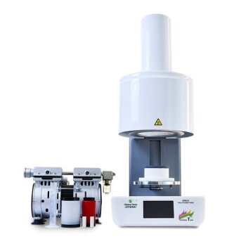
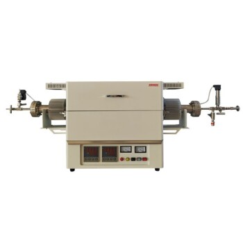
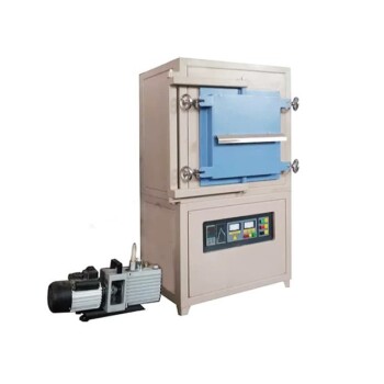
Unlock advanced material consolidation with KINTEK's cutting-edge laboratory high-temperature furnaces. Whether you are scaling up field-assisted sintering, exploring mixed-conducting oxides, or engineering next-generation ceramics, our high-temperature furnace systems—including specialized vacuum, atmosphere, tube, muffle, and customizable high-current solutions—provide the ultra-precise control you need.
Reduce thermal budgets, refine grain microstructures, and achieve superior densification rates. Contact KINTEK today to speak with our thermal equipment experts and configure the ideal furnace for your research or manufacturing requirements!
Related Products
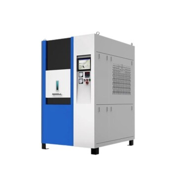
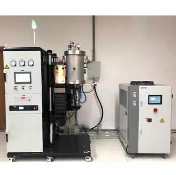
- Spark Plasma Sintering SPS Furnace
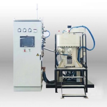
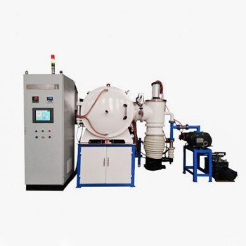
- 9MPa Air Pressure Vacuum Heat Treat and Sintering Furnace
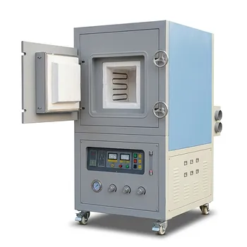
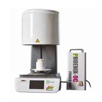
- High Temperature Muffle Oven Furnace for Laboratory Debinding and Pre Sintering
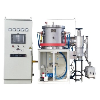
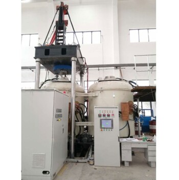
- 2200 ℃ Tungsten Vacuum Heat Treat and Sintering Furnace
- Vacuum Heat Treat Sintering Furnace Molybdenum Wire Vacuum Sintering Furnace
People Also Ask
- Why is it necessary to maintain a high vacuum environment during the SPS of SiC? Key to High-Density Ceramics
- How does the heating mechanism of Spark Plasma Sintering (SPS) function? Enhance TiC/SiC Composite Fabrication
- What are the technical advantages of using an SPS sintering furnace? Elevate Al2O3-TiC Material Performance
- What are the steps in the discharge plasma sintering process? Master Fast, High-Density Material Consolidation
- What are the advantages of spark plasma sintering (SPS) over traditional forging? Precision Microstructural Control