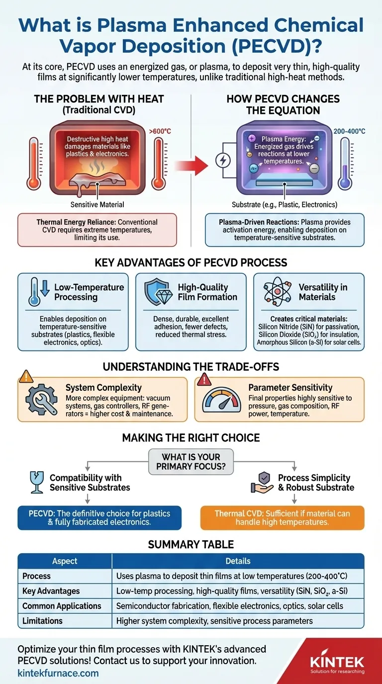
At its core, Plasma Enhanced Chemical Vapor Deposition (PECVD) is a process used to deposit very thin, high-quality films of material onto a substrate. Unlike traditional methods that require intense heat, PECVD uses an energized gas, or plasma, to drive the chemical reactions. This fundamental difference allows for deposition at significantly lower temperatures, making it indispensable in modern manufacturing.
The central challenge in thin film deposition is achieving a durable, high-quality coating without damaging the underlying material. PECVD solves this by using the energy of a plasma to replace the destructive, high heat of conventional methods, enabling advanced fabrication on temperature-sensitive substrates.
The Problem with Heat in Deposition
Traditional Chemical Vapor Deposition (CVD) is a powerful technique, but it has a significant limitation: it relies almost exclusively on thermal energy.
The Thermal CVD Process
In a conventional CVD process, a substrate is heated to very high temperatures (often >600°C). Precursor gases are then introduced into the chamber, and the heat from the substrate provides the energy needed to break them down and cause them to react, forming a solid film on the surface.
The Temperature Limitation
This reliance on high heat means conventional CVD cannot be used on materials that would melt, warp, or be otherwise damaged by the extreme temperatures. This includes many plastics, certain electronic components, and other advanced materials critical for modern devices.
How PECVD Changes the Equation
PECVD overcomes the heat limitation by introducing a new source of energy: plasma. This allows it to achieve similar, and often superior, results at much lower temperatures (typically 200-400°C).
The Role of Plasma Energy
A plasma is a state of matter where a gas is energized, causing it to ionize and create a mix of ions, electrons, and neutral particles. In PECVD, an electric field is applied to a low-pressure gas, creating this plasma.
The highly energetic electrons within the plasma collide with the precursor gas molecules. These collisions transfer energy, breaking the chemical bonds and creating reactive species without needing high thermal energy from the substrate.
The Deposition Process
These newly created reactive gas species then travel to the comparatively cool substrate, where they adsorb and form a high-quality, solid thin film. The plasma essentially provides the activation energy for the reaction that heat would normally provide.
Key Advantages of the PECVD Process
Using plasma instead of high heat unlocks several critical advantages that have made PECVD a cornerstone of the semiconductor and materials science industries.
Low-Temperature Processing
This is the primary advantage of PECVD. It enables the deposition of films on temperature-sensitive substrates, dramatically expanding the range of possible applications in fields from flexible electronics to optics.
High-Quality Film Formation
PECVD films are known for being dense, durable, and having excellent adhesion. The process reduces thermal stress between the film and substrate, resulting in stronger bonding and fewer defects like pinholes.
Versatility in Materials
The process is used to create some of the most important materials in microfabrication. Common films include silicon nitride (SiN) for passivation and masking, **silicon dioxide (SiO₂) ** for electrical insulation, and amorphous silicon (a-Si) for solar cells and transistors.
Understanding the Trade-offs
While powerful, PECVD is not without its complexities. Objectively understanding its limitations is key to using it effectively.
System Complexity
A PECVD system is more complex than a simple thermal CVD reactor. It requires sophisticated vacuum systems, precise gas flow controllers, and RF power generators to create and sustain the plasma, increasing initial cost and maintenance.
Parameter Sensitivity
The final properties of the deposited film are extremely sensitive to a wide range of process parameters. Variables like pressure, gas composition, RF power, and temperature must be meticulously controlled and optimized to achieve reproducible, high-quality results.
Making the Right Choice for Your Goal
Selecting a deposition method depends entirely on your project's constraints and desired outcome. PECVD is a specialized tool that excels in specific, critical scenarios.
- If your primary focus is compatibility with sensitive substrates: PECVD is the definitive choice for depositing films on plastics, fully fabricated electronics, or other materials that cannot withstand high heat.
- If your primary focus is high-quality dielectric films: PECVD excels at creating dense, durable, and low-stress passivation or insulation layers like silicon nitride and silicon dioxide for semiconductor devices.
- If your primary focus is process simplicity and your substrate is robust: A simpler thermal CVD process may be sufficient, provided your material can handle the required temperatures without damage.
By substituting targeted plasma energy for brute-force heat, PECVD enables the creation of the advanced materials that power our technological world.
Summary Table:
| Aspect | Details |
|---|---|
| Process | Uses plasma to deposit thin films at low temperatures (200-400°C) |
| Key Advantages | Low-temperature processing, high-quality films, versatility in materials (e.g., SiN, SiO₂, a-Si) |
| Common Applications | Semiconductor fabrication, flexible electronics, optics, solar cells |
| Limitations | Higher system complexity, sensitive process parameters |
Optimize your thin film processes with KINTEK's advanced PECVD solutions! Leveraging exceptional R&D and in-house manufacturing, we provide diverse laboratories with high-temperature furnace systems like CVD/PECVD, Muffle, Tube, Rotary, and Vacuum & Atmosphere Furnaces. Our strong deep customization capability ensures precise solutions for your unique experimental needs, enhancing efficiency and performance. Contact us today to discuss how we can support your innovation!
Visual Guide
Related Products
- Slide PECVD Tube Furnace with Liquid Gasifier PECVD Machine
- RF PECVD System Radio Frequency Plasma Enhanced Chemical Vapor Deposition
- Inclined Rotary Plasma Enhanced Chemical Deposition PECVD Tube Furnace Machine
- Inclined Rotary Plasma Enhanced Chemical Deposition PECVD Tube Furnace Machine
- Multi Heating Zones CVD Tube Furnace Machine for Chemical Vapor Deposition Equipment
People Also Ask
- In which industries is the tube furnace commonly used? Essential for Materials Science, Energy, and More
- What is plasma in the context of PECVD? Unlock Low-Temperature Thin Film Deposition
- What are the main advantages of PECVD tube furnaces compared to CVD tube furnaces? Lower Temp, Faster Deposition, and More
- How does a hydrogen reduction environment in an industrial tube furnace facilitate gold-copper alloy microspheres?
- What are the advantages of using a tube furnace CVD system for Cu(111)/graphene? Superior Scalability and Quality


