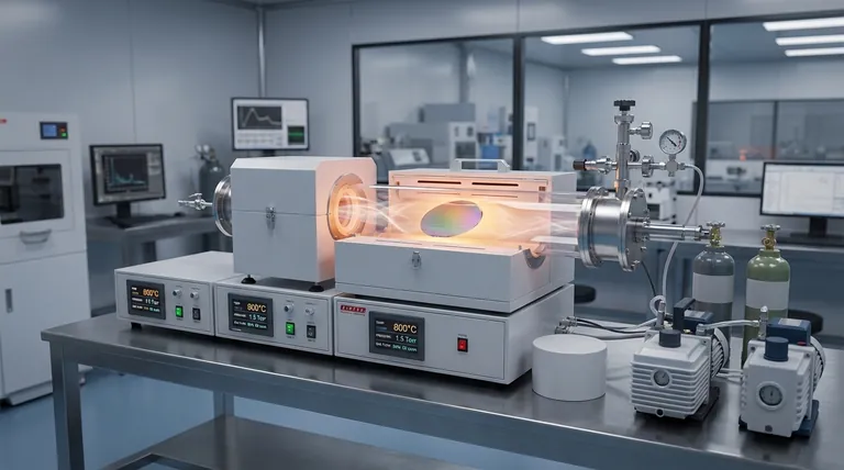
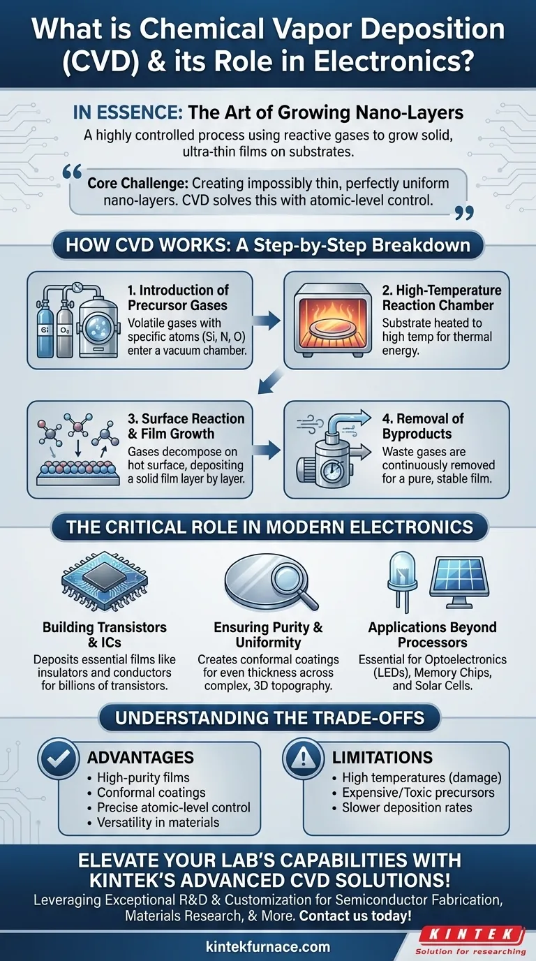
In essence, Chemical Vapor Deposition (CVD) is a highly controlled manufacturing process where reactive gases are used to grow a solid, ultra-thin film of material onto a surface, or substrate. In electronics manufacturing, this is not just an important process; it is the fundamental method used to construct the microscopic layers that form the building blocks of virtually all modern semiconductor devices, including transistors and integrated circuits.
The core challenge in modern electronics is creating impossibly thin, perfectly uniform material layers at a nano-scale. CVD solves this by using controlled chemical reactions in a gas phase, allowing engineers to "grow" these precise films with atomic-level control onto a substrate like a silicon wafer.
How Chemical Vapor Deposition Works: A Step-by-Step Breakdown
To understand why CVD is so critical, you must first understand its mechanism. The process is a carefully orchestrated sequence of events inside a highly controlled reaction chamber.
Introduction of Precursor Gases
The process begins by introducing one or more volatile gases, known as precursors, into a vacuum chamber. These gases contain the specific atoms (e.g., silicon, nitrogen, oxygen) required to form the desired solid film.
The High-Temperature Reaction Chamber
The substrate, typically a silicon wafer, is heated to a precise and often very high temperature inside the chamber. This heat provides the necessary thermal energy to initiate a chemical reaction.
Surface Reaction and Film Growth
When the precursor gas molecules come into contact with the hot substrate, they decompose and react. This chemical reaction results in the formation of a solid material that deposits directly onto the substrate's surface, building up the film layer by layer.
Removal of Byproducts
The chemical reactions also produce gaseous byproducts, which are not part of the final film. These waste gases are continuously removed from the chamber by the vacuum system, leaving behind a pure and stable thin film.
The Critical Role of CVD in Modern Electronics
CVD isn't just one of many techniques; it's a cornerstone of the semiconductor industry. Its ability to create high-purity, uniform films is directly responsible for the performance and miniaturization of modern electronics.
Building Transistors and Integrated Circuits
A modern transistor has multiple layers, including conductive gates, insulating dielectric layers, and semiconducting channels. CVD is used to deposit many of these essential films, such as silicon dioxide (an insulator) or polycrystalline silicon (a conductor), with the precision required for a device containing billions of transistors.
Ensuring Purity and Uniformity
The performance of a microchip is extremely sensitive to impurities or variations in layer thickness. CVD excels at producing conformal coatings, meaning the film's thickness is perfectly even across the entire complex, three-dimensional topography of a wafer. This ensures every single transistor performs reliably.
Applications Beyond Processors
The utility of CVD extends beyond just CPUs. It is essential for manufacturing optoelectronics (like LEDs), memory chips, and the transparent conductive oxides used in printable solar cells and display panels.
Understanding the Trade-offs
While powerful, CVD is not a universal solution. As a technical advisor, it's crucial to recognize its operational realities and limitations.
The Need for High Temperatures
Traditional CVD processes require very high temperatures, which can sometimes damage or alter previously deposited layers on a complex chip. This has led to the development of variants like Plasma-Enhanced CVD (PECVD), which can operate at lower temperatures.
Precursor Material Costs and Safety
The specialized precursor gases used in CVD can be expensive, toxic, or pyrophoric (igniting on contact with air). Handling these materials requires significant investment in safety infrastructure and protocols, adding to the overall cost of fabrication.
Deposition Rate vs. Quality
CVD is renowned for quality, not speed. The process of growing a film atom-by-atom can be slower compared to physical deposition methods. For applications where ultimate purity and uniformity are less critical, other methods may be chosen to increase manufacturing throughput.
Making the Right Choice for Your Goal
Understanding the principles of CVD allows you to appreciate its role in different contexts.
- If your primary focus is fabricating high-performance semiconductors: CVD is non-negotiable for creating the ultra-pure, uniform dielectric and conductive films required for the critical layers of modern transistors.
- If your primary focus is developing novel materials: CVD offers unmatched control over film composition and structure, making it the ideal process for R&D in areas like advanced coatings, energy storage, or catalysis.
- If your primary focus is optimizing manufacturing cost: You must evaluate the high-quality output of CVD against its operational costs (energy, precursor gases) and consider alternative deposition methods for less critical layers where speed is a priority.
Ultimately, understanding Chemical Vapor Deposition is to understand the fundamental construction process behind the entire digital world.
Summary Table:
| Aspect | Key Details |
|---|---|
| Process Overview | Uses reactive gases to grow solid thin films on substrates via controlled chemical reactions in a vacuum chamber. |
| Key Steps | 1. Introduce precursor gases 2. Heat substrate 3. Surface reaction and film growth 4. Remove byproducts |
| Role in Electronics | Essential for building transistors, ICs, LEDs, and memory chips; ensures purity and uniformity at nano-scale. |
| Advantages | High-purity films, conformal coatings, precise atomic-level control, versatility in materials. |
| Limitations | High temperatures, expensive/toxic precursors, slower deposition rates compared to other methods. |
| Applications | Semiconductors, optoelectronics, solar cells, R&D for advanced coatings and energy storage. |
Elevate your lab's capabilities with KINTEK's advanced CVD solutions! Leveraging exceptional R&D and in-house manufacturing, we provide diverse laboratories with high-temperature furnace systems like CVD/PECVD, Muffle, Tube, Rotary, Vacuum & Atmosphere Furnaces. Our strong deep customization ensures precise alignment with your unique experimental needs in semiconductor fabrication, materials research, and beyond. Contact us today to discuss how our tailored solutions can drive your innovations forward!
Visual Guide
Related Products
- RF PECVD System Radio Frequency Plasma Enhanced Chemical Vapor Deposition
- 915MHz MPCVD Diamond Machine Microwave Plasma Chemical Vapor Deposition System Reactor
- MPCVD Machine System Reactor Bell-jar Resonator for Lab and Diamond Growth
- Custom Made Versatile CVD Tube Furnace Chemical Vapor Deposition CVD Equipment Machine
- HFCVD Machine System Equipment for Drawing Die Nano Diamond Coating
People Also Ask
- How does film quality compare between PECVD and CVD? Choose the Best Method for Your Substrate
- How are deposition rates and film properties controlled in PECVD? Master Key Parameters for Optimal Thin Films
- What are the key advantages of PECVD technology? Achieve Low-Temperature, High-Quality Thin Film Deposition
- What is PECVD specification? A Guide to Choosing the Right System for Your Lab
- What is RF in PECVD? A Critical Control for Plasma Deposition


