At its core, Chemical Vapor Deposition (CVD) is a highly controlled process for manufacturing high-performance solid materials, typically as a thin film on a surface. It achieves this by introducing precursor gases into a chamber, which then react and decompose on a heated substrate to form a new solid layer. Its primary industrial application is in the semiconductor industry for the fabrication of integrated circuits, the foundational components of all modern electronics.
CVD is not merely a coating technique; it is a bottom-up manufacturing process. It allows engineers to build materials atom by atom, enabling the creation of the ultra-pure, perfectly structured thin films required for high-performance microelectronics and advanced materials.
How CVD Works: Building from the Vapor Up
CVD is a thermochemical process that relies on precision control over the environment to construct new materials from gaseous building blocks.
The Core Principle: Chemical Reaction
The process takes place within a vacuum chamber to ensure purity. One or more volatile precursor gases, which contain the elements you want to deposit, are introduced into the chamber.
Unlike physical coating methods (like spray painting), CVD does not simply transfer an existing material. It creates a new solid material directly on the target surface through a chemical reaction.
The Role of the Substrate
The object to be coated, known as the substrate, is heated to a specific, often high, temperature. This heat provides the necessary energy to trigger the chemical reactions in the precursor gases.
The reactions occur primarily on the hot surface of the substrate, causing the desired solid material to "deposit" and form a film.
Formation of the Solid Film
As the precursor gases decompose and react, they form a non-volatile solid that bonds to the substrate. This deposition occurs molecule by molecule, resulting in a very dense, pure, and high-performance film.
By-product gases from the reaction are simply pumped out of the vacuum chamber, leaving only the desired thin film behind.
Creating Conformal Coatings
A key advantage of CVD is its ability to create conformal films. Because the precursor is a gas, it can reach every nook and cranny of a complex, three-dimensional surface.
This ensures the deposited film has a uniform thickness across the entire object, which is impossible to achieve with line-of-sight techniques like spraying or Physical Vapor Deposition (PVD).
The Primary Application: Fabricating Microelectronics
While CVD has many uses, its impact is most profound in the semiconductor industry. Without it, modern computing would not exist.
Building Integrated Circuits (ICs)
Microchips are not carved from a single block; they are built up in dozens or even hundreds of layers. CVD is the workhorse process used to deposit many of these critical layers.
These layers can be insulating (dielectrics), conducting (metals), or semiconducting, forming the microscopic transistors, wires, and gates that make up a processor or memory chip.
Unmatched Precision and Purity
The performance of a microchip depends on the absolute purity and structural perfection of its layers.
Because CVD builds films atom by atom, it provides the exceptional control needed to create these defect-free layers, which can be just a few nanometers thick.
Beyond Integrated Circuits
The versatility of CVD extends to many other high-tech fields. It is used to create:
- Wear-resistant coatings on cutting tools and engine parts to dramatically increase their lifespan.
- Highly efficient layers in photovoltaic devices (solar cells).
- Specialized sensors for consumer electronics, automotive systems, and medical biosensors.
- Advanced membranes for water treatment and gas separation.
Understanding the Trade-offs
CVD is a powerful tool, but its advantages come with specific requirements and limitations.
High Temperature and Vacuum
Most CVD processes require high temperatures and a high-vacuum environment. This necessitates complex, expensive equipment and high energy consumption.
Precursor Chemistry
The choice of precursor gases is critical. They can be toxic, flammable, or corrosive, requiring stringent safety protocols. The cost and availability of high-purity precursors are also significant factors.
Deposition Rate vs. Quality
CVD is known for its exceptional quality, but the deposition rate can be slower than other methods. This represents a classic engineering trade-off between manufacturing speed and the performance of the final product.
Making the Right Choice for Your Goal
Deciding whether to use CVD depends entirely on the technical requirements of your application.
- If your primary focus is creating ultra-pure, defect-free layers for microelectronics: CVD is the industry standard and the only viable choice for achieving atomic-level precision.
- If your primary focus is applying a durable, uniform coating on complex 3D shapes: CVD's ability to create conformal films makes it a superior choice for parts requiring complete and even coverage.
- If your primary focus is low-cost, rapid coating of simple surfaces where microscopic perfection is not required: Alternatives like PVD or spray coating may be more cost-effective, as the complexity of CVD would be unnecessary.
Ultimately, Chemical Vapor Deposition is a foundational technology that enables the creation of materials that would otherwise be impossible to make, forming the bedrock of modern high-performance devices.
Summary Table:
| Aspect | Description |
|---|---|
| Process | Chemical reaction in a vacuum chamber using precursor gases to deposit solid films on a heated substrate |
| Key Feature | Conformal coatings with uniform thickness on complex 3D surfaces |
| Primary Application | Semiconductor industry for integrated circuits (ICs) |
| Other Uses | Wear-resistant coatings, solar cells, sensors, and membranes |
| Advantages | High purity, defect-free layers, precise atomic control |
| Limitations | High temperature, vacuum requirements, slower deposition rates |
Ready to enhance your lab's capabilities with tailored CVD solutions? KINTEK leverages exceptional R&D and in-house manufacturing to provide advanced high-temperature furnace systems, including CVD/PECVD Systems, Muffle, Tube, Rotary Furnaces, and Vacuum & Atmosphere Furnaces. Our strong deep customization capability ensures we precisely meet your unique experimental needs for semiconductor fabrication, wear-resistant coatings, and more. Contact us today to discuss how our solutions can drive your innovations forward!
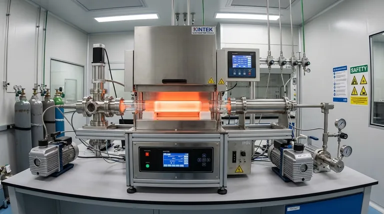
Visual Guide

Related Products
- Custom Made Versatile CVD Tube Furnace Chemical Vapor Deposition CVD Equipment Machine
- HFCVD Machine System Equipment for Drawing Die Nano Diamond Coating
- Multi Heating Zones CVD Tube Furnace Machine for Chemical Vapor Deposition Equipment
- MPCVD Machine System Reactor Bell-jar Resonator for Lab and Diamond Growth
- 915MHz MPCVD Diamond Machine Microwave Plasma Chemical Vapor Deposition System Reactor
People Also Ask
- What is the working principle of a CVD tube furnace? Achieve Precise Thin Film Deposition for Your Lab
- What improvements can be made to the bonding force of gate dielectric films using a CVD tube furnace? Enhance Adhesion for Reliable Devices
- What are the key features of CVD tube furnaces for 2D material processing? Unlock Precision Synthesis for Superior Materials
- How can integrating CVD tube furnaces with other technologies benefit device fabrication? Unlock Advanced Hybrid Processes
- Which industries and research fields benefit from CVD tube furnace sintering systems for 2D materials? Unlock Next-Gen Tech Innovations