In essence, Chemical Vapor Deposition (CVD) is a sophisticated manufacturing process that builds a high-performance, solid thin film on a surface from a gas. Gaseous molecules, known as precursors, are introduced into a reaction chamber where they are energized, typically by heat. This energy causes chemical reactions that deposit a thin, pure, and highly controlled layer of material onto a target object, or substrate.
The core challenge in advanced manufacturing is creating flawlessly pure, uniform thin films that are the foundation of modern electronics and high-performance materials. CVD solves this not by simply "coating" a surface, but by chemically constructing a new layer atom by atom, enabling a level of precision and quality that other methods cannot achieve.
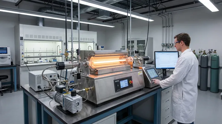
How CVD Works: From Gas to Solid Film
CVD is best understood as a highly controlled chemical construction process occurring at a microscopic scale. The entire operation happens within a sealed reaction chamber to ensure purity and control.
The Role of Precursors
Precursors are the gaseous "building blocks" of the film. They are carefully selected chemical compounds in a vapor state that contain the specific elements needed for the final coating.
These gases are precisely metered and fed into the reaction chamber. The continuous flow ensures a consistent supply of material for the deposition reaction.
The Reaction Chamber and Substrate
The substrate is the object that will be coated. It is placed inside the reaction chamber, which can be held under vacuum or at a specific atmospheric pressure.
This controlled environment is critical for preventing contamination from unwanted particles or gases, which would compromise the quality and purity of the final film.
The Energy Trigger
Energy is required to break the chemical bonds in the precursor gases and initiate the deposition reaction. Most commonly, this energy is high temperature (thermal CVD).
The substrate is heated, and when the hot precursor gases come into contact with the heated surface, they decompose or react. Other energy sources, like plasma (PECVD) or light, can be used to drive these reactions, often at lower temperatures.
Deposition and Film Growth
As the precursor gases react on the substrate's surface, they form a new, stable, solid material. This material deposits onto the substrate, creating a thin film.
The process is meticulously controlled, allowing the film to grow with a specific thickness, uniformity, and composition. The duration of the process and the concentration of precursor gases are the primary levers for controlling film thickness.
Managing By-products
The chemical reactions that form the solid film also produce gaseous by-products. These waste gases are continuously removed from the reaction chamber by a vacuum or exhaust system.
Removing by-products is essential to maintain the purity of the reaction and prevent them from being incorporated as defects into the growing film.
Why CVD is Critical for Modern Technology
CVD is not just one of many coating techniques; it is a foundational process that enables the performance of many advanced products. Its unique advantages make it indispensable in several high-tech industries.
Unmatched Purity and Quality
Because the film is built from a purified gaseous state, CVD can produce films of exceptionally high purity and structural quality. This is vital for applications like semiconductors, where even microscopic impurities can cause device failure.
Conformal Coverage
One of CVD's most significant advantages is its ability to create conformal coatings. The precursor gas flows around the substrate, allowing the film to deposit evenly over complex, three-dimensional shapes and inside deep trenches. This is a distinct advantage over line-of-sight methods like sputtering.
A Foundation for Semiconductors
The modern microchip would not exist without CVD. It is used to deposit the critical layers of silicon, silicon dioxide, and other materials that form the transistors and wiring in integrated circuits.
Protective and Functional Coatings
Beyond electronics, CVD is used to apply extremely hard and durable coatings to industrial tools, machine parts, and medical implants. These films provide exceptional resistance to wear, corrosion, and high temperatures, dramatically extending the life and performance of the underlying part.
Understanding the Trade-offs
While powerful, CVD is not a universal solution. Understanding its limitations is key to using it effectively.
High Temperature Requirements
Traditional thermal CVD processes often require very high temperatures (several hundred to over a thousand degrees Celsius). This can damage or destroy substrates that are not thermally stable, such as polymers or certain metals.
Precursor Chemistry and Safety
The precursor gases used in CVD can be highly toxic, flammable, or corrosive. This necessitates complex and expensive safety protocols, gas handling systems, and exhaust management.
Process Complexity and Cost
CVD systems are sophisticated pieces of equipment that require significant capital investment and operational expertise. The complexity and cost make it best suited for high-value applications where performance justifies the expense.
Process Variants
To overcome these limitations, several variations of CVD have been developed. Plasma-Enhanced CVD (PECVD), for example, uses plasma to energize the reaction, allowing deposition to occur at much lower temperatures, making it suitable for sensitive substrates.
Making the Right Choice for Your Goal
Selecting the right deposition technology depends entirely on your material requirements and substrate limitations.
- If your primary focus is manufacturing the highest-purity semiconductor layers: Traditional thermal CVD is the industry standard for creating the foundational electronic materials of microchips.
- If your primary focus is applying a hard, wear-resistant coating on robust tools: High-temperature CVD is the ideal choice for creating extremely durable protective films on thermally stable metal substrates.
- If your primary focus is coating temperature-sensitive materials like plastics or electronics: A lower-temperature variant like Plasma-Enhanced CVD (PECVD) is the necessary approach to avoid damaging the substrate.
Ultimately, Chemical Vapor Deposition is a cornerstone of modern materials engineering, empowering us to build advanced materials from the atoms up.
Summary Table:
| Aspect | Key Details |
|---|---|
| Process | Builds solid thin films from gas precursors via chemical reactions in a controlled chamber. |
| Key Advantages | High purity, conformal coverage, precise control over film properties. |
| Common Applications | Semiconductors, protective coatings, medical implants, industrial tools. |
| Limitations | High temperatures, complex safety protocols, high cost. |
| Variants | Includes Plasma-Enhanced CVD (PECVD) for lower-temperature processes. |
Ready to elevate your laboratory's capabilities with advanced high-temperature furnace solutions? At KINTEK, we leverage exceptional R&D and in-house manufacturing to provide diverse labs with cutting-edge equipment like Muffle, Tube, Rotary Furnaces, Vacuum & Atmosphere Furnaces, and CVD/PECVD Systems. Our strong deep customization capability ensures we can precisely meet your unique experimental requirements, delivering high-purity, uniform thin films for applications in semiconductors, coatings, and beyond. Don't let process limitations hold you back—contact us today to discuss how our tailored solutions can drive your innovation and efficiency!
Visual Guide

Related Products
- Custom Made Versatile CVD Tube Furnace Chemical Vapor Deposition CVD Equipment Machine
- Multi Heating Zones CVD Tube Furnace Machine for Chemical Vapor Deposition Equipment
- HFCVD Machine System Equipment for Drawing Die Nano Diamond Coating
- Split Chamber CVD Tube Furnace with Vacuum Station CVD Machine
- 915MHz MPCVD Diamond Machine Microwave Plasma Chemical Vapor Deposition System Reactor
People Also Ask
- What improvements can be made to the bonding force of gate dielectric films using a CVD tube furnace? Enhance Adhesion for Reliable Devices
- What are the key application fields of CVD tube furnaces? Unlock Precision in Thin-Film Synthesis
- How might AI and machine learning enhance CVD tube furnace processes? Boost Quality, Speed, and Safety
- What are the key features of CVD tube furnaces for 2D material processing? Unlock Precision Synthesis for Superior Materials
- What is a CVD tube furnace and what is its primary function? Discover Precision Thin-Film Deposition


