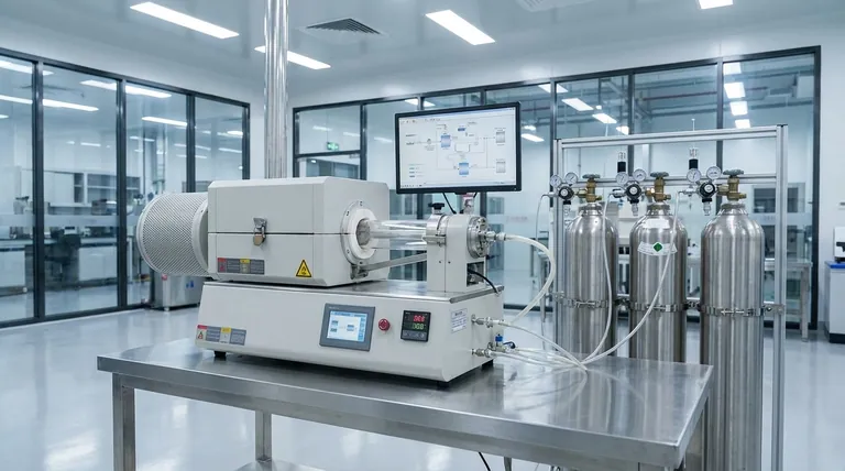
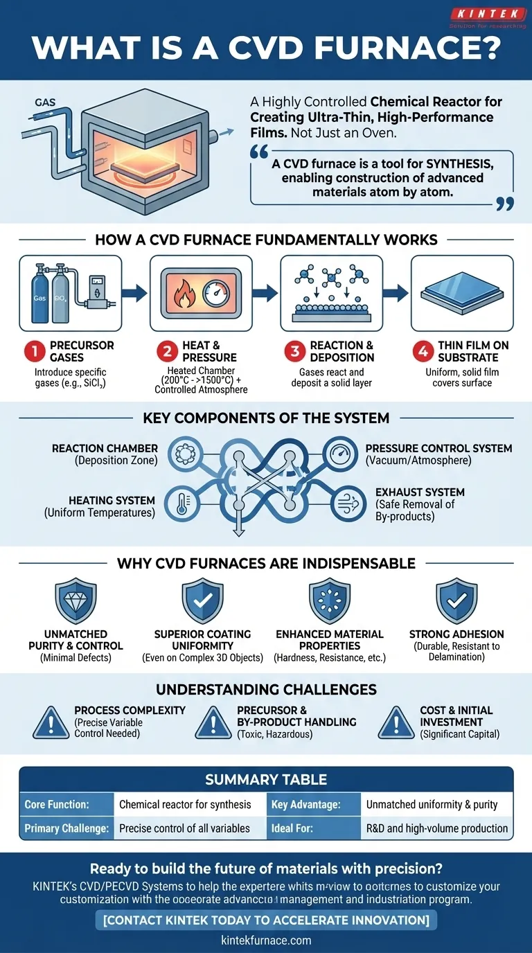
At its core, a Chemical Vapor Deposition (CVD) furnace is a highly controlled chemical reactor, not just a simple oven. It is specialized equipment designed to create ultra-thin, high-performance films or coatings on a surface, known as a substrate. This is achieved by introducing specific gases (precursors) into a heated chamber, which then react and deposit a solid layer, atom by atom, onto the target material.
The crucial insight is that a CVD furnace is a tool for synthesis, not just heating. It enables the construction of advanced materials with precisely engineered properties—such as hardness, purity, and thermal resistance—by building them from a gaseous chemical state.
How a CVD Furnace Fundamentally Works
Understanding a CVD furnace requires seeing it as a complete system where temperature, pressure, and chemistry are meticulously managed to build a new material.
The Core Principle: Chemical Vapor Deposition
The process begins by introducing one or more volatile precursor gases into a reaction chamber. For example, to create a silicon-based coating, a gas like methyltrichlorosilane (CH₃SiCl₃) might be used.
The Role of Heat and Pressure
The chamber is heated to a precise, high temperature, often ranging from 200°C to over 1500°C. This intense heat provides the energy needed for the precursor gases to decompose or react with each other. The environment is also controlled, operating under vacuum, low pressure, or at atmospheric pressure depending on the desired outcome.
The Deposition Process
As the gases react, they form a solid material that condenses and deposits onto the surface of the substrate placed inside the furnace. This builds up a thin, solid film. Because the deposition happens from a gas, the film can be incredibly uniform, covering even complex and intricate shapes evenly.
Key Components of the System
A CVD furnace is more than its chamber. It is an integrated system comprising:
- A Reaction Chamber: The furnace tube or enclosure where the deposition occurs.
- A Heating System: Provides uniform, high temperatures.
- A Gas Delivery System: Precisely controls the flow rates of precursor gases.
- A Pressure Control System: Manages the atmosphere inside the chamber, often using vacuum pumps.
- An Exhaust System: Safely removes unreacted gases and toxic by-products.
Why CVD Furnaces are Indispensable
The unique capabilities of the CVD process make these furnaces a cornerstone technology in many advanced industries, from semiconductors to aerospace.
Unmatched Purity and Control
Because the process builds materials from purified chemical vapors, the resulting films have exceptionally high purity with minimal defects. This level of control is critical for applications like manufacturing microchips.
Superior Coating Uniformity
Unlike liquid-based coating methods, the gaseous precursors can reach every part of a substrate's surface. This ensures a consistent and uniform coating thickness, even on complex 3D objects.
Enhanced Material Properties
CVD coatings can drastically improve a material's performance. They are used to add hardness, increase corrosion resistance, provide thermal stability, or alter optical and electrical characteristics.
Strong Adhesion
The chemical bonding that occurs during deposition results in films that adhere exceptionally well to the substrate, making them durable and resistant to delamination.
Understanding the Trade-offs and Challenges
While powerful, the CVD process is not without its complexities. Objectivity requires acknowledging its operational demands and limitations.
Process Complexity
Achieving a high-quality, repeatable result depends on the precise and stable control of multiple variables: temperature, pressure, gas flow rates, and chemistry. Small deviations can significantly impact the final material's properties.
Precursor and By-product Handling
Many precursor gases used in CVD are toxic, flammable, or corrosive. Likewise, the chemical reactions often produce hazardous by-products. This necessitates sophisticated safety protocols and efficient exhaust and scrubbing systems.
Cost and Initial Investment
CVD systems, particularly those for industrial-scale production, represent a significant capital investment. The complexity of the equipment and the need for robust safety infrastructure contribute to the overall cost.
Laboratory vs. Industrial Scale
The requirements for a research lab furnace differ greatly from one used in mass production. Lab furnaces prioritize flexibility, modular design, and adaptability for various experiments. Industrial furnaces prioritize throughput, automation, and unwavering process consistency.
Making the Right Choice for Your Goal
Selecting or specifying a CVD furnace requires a clear understanding of your primary objective.
- If your primary focus is research and development: Prioritize a modular system with precise, adaptable controls to accommodate a wide range of materials and experiments.
- If your primary focus is high-volume industrial production: Emphasize scalability, process automation, robust safety systems, and consistent uniformity for mass manufacturing.
- If your primary focus is creating highly specialized materials: Focus on a furnace with advanced gas delivery and temperature profiling to precisely tune the coating's final properties.
Ultimately, mastering the CVD process comes from understanding that the furnace is a precision instrument for building materials from the ground up.
Summary Table:
| Key Aspect | Description |
|---|---|
| Core Function | A chemical reactor for synthesizing thin films via gas-phase reactions. |
| Key Advantage | Unmatched coating uniformity, purity, and material property enhancement. |
| Primary Challenge | Requires precise control of temperature, pressure, and gas chemistry. |
| Ideal For | R&D of new materials and high-volume production of advanced components. |
Ready to build the future of materials with precision?
Leveraging exceptional R&D and in-house manufacturing, KINTEK provides diverse laboratories with advanced high-temperature furnace solutions. Our CVD/PECVD Systems are engineered for unparalleled control, enabling you to synthesize advanced materials with precisely engineered properties.
Our strong deep customization capability ensures your furnace precisely meets your unique experimental or production requirements, whether for flexible R&D or high-volume industrial scaling.
Contact KINTEK today to discuss how our tailored CVD furnace solutions can accelerate your innovation.
Visual Guide
Related Products
- Custom Made Versatile CVD Tube Furnace Chemical Vapor Deposition CVD Equipment Machine
- Split Chamber CVD Tube Furnace with Vacuum Station CVD Machine
- Multi Heating Zones CVD Tube Furnace Machine for Chemical Vapor Deposition Equipment
- Slide PECVD Tube Furnace with Liquid Gasifier PECVD Machine
- Controlled Inert Nitrogen Hydrogen Atmosphere Furnace
People Also Ask
- How can integrating CVD tube furnaces with other technologies benefit device fabrication? Unlock Advanced Hybrid Processes
- What are the key features of CVD tube furnaces for 2D material processing? Unlock Precision Synthesis for Superior Materials
- What is a CVD tube furnace and what is its primary function? Discover Precision Thin-Film Deposition
- Why are CVD tube furnace sintering systems indispensable for 2D material research and production? Unlock Atomic-Scale Precision
- How does CVD tube furnace sintering enhance graphene growth? Achieve Superior Crystallinity and High Electron Mobility


