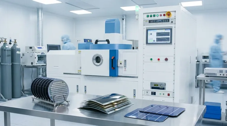
At its core, the market growth for Plasma-Enhanced Chemical Vapor Deposition (PECVD) is driven by its unique ability to deposit high-quality, uniform thin films at significantly lower temperatures than traditional methods. This capability is indispensable for manufacturing modern electronics, solar cells, and advanced materials where heat would damage the underlying components. The relentless demand for smaller, more powerful semiconductors and more efficient renewable energy technologies directly fuels the adoption of PECVD.
The fundamental driver for PECVD is not just what it does—deposit thin films—but how it does it. By using an energy-rich plasma instead of high heat, it unlocks manufacturing possibilities for heat-sensitive, complex devices that are at the heart of today's fastest-growing technology sectors.
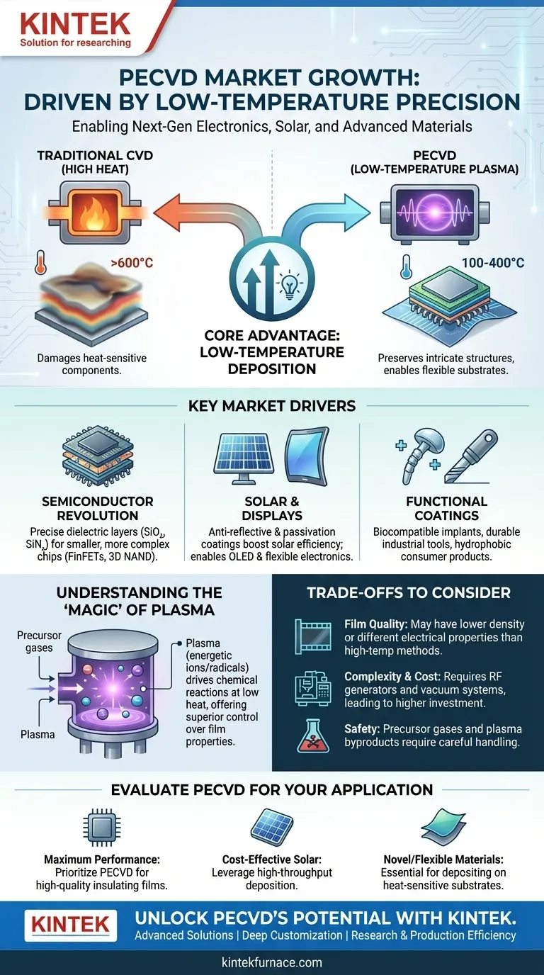
The Core Advantage: Low-Temperature Deposition
The defining characteristic of PECVD is its low-temperature operation, typically in the 100-400°C range. This contrasts sharply with traditional Chemical Vapor Deposition (CVD), which can require temperatures of 600-900°C or higher.
Why Low Temperature Matters
In fabricating multi-layered integrated circuits, high temperatures can cause previously deposited layers to diffuse, change their properties, or become damaged. PECVD’s low thermal budget preserves the integrity of these intricate structures, making it essential for advanced semiconductor manufacturing.
Enabling Advanced Substrates
This low-temperature process allows for deposition on a wide variety of materials that cannot withstand high heat. This includes polymers, plastics, and other flexible substrates, opening the door for applications like flexible electronics, OLED displays, and specialized optical coatings.
Key Market Drivers Fueled by PECVD's Capabilities
PECVD's technical advantages directly translate into solutions for the biggest challenges in several high-growth industries.
The Semiconductor Revolution
As microchips become smaller and more complex (e.g., FinFETs, 3D NAND), the need for precise, low-temperature film deposition becomes critical. PECVD is the workhorse technology for depositing essential dielectric layers, such as silicon dioxide (SiO₂) and silicon nitride (SiNₓ), which are used for insulation, passivation, and encapsulation.
The Rise of Solar and Displays
In solar cell manufacturing, PECVD is used to deposit silicon nitride anti-reflective coatings and passivation layers. These films dramatically increase the amount of light the cell can absorb and convert into electricity, directly boosting efficiency and making solar energy more competitive.
Protective and Functional Coatings
Beyond electronics, PECVD is used to create highly durable and specialized coatings. This includes biocompatible coatings for medical implants, wear-resistant layers for industrial tools, and hydrophobic coatings for consumer products.
Understanding the Technical Nuances
The "magic" of PECVD lies in its use of plasma to drive the chemical reaction.
The Role of Plasma
Instead of relying on thermal energy to break apart precursor gases, PECVD uses an electromagnetic field (typically radio frequency) to create a plasma. This plasma is a highly energetic state of matter containing ions and radicals that are far more reactive than the initial gas molecules.
Control and Flexibility
This plasma-based process provides exceptional control. As the reference material notes, by adjusting plasma density and other parameters, engineers can fine-tune the properties of the deposited film, such as its density, stress, and optical index. Operating at lower pressures also improves the directionality of the film deposition, which is critical for coating complex 3D structures uniformly.
Understanding the Trade-offs
While powerful, PECVD is not a universal solution. Understanding its limitations is key to making an informed decision.
Film Quality Considerations
PECVD films often incorporate hydrogen or other byproducts from the precursor gases, which can sometimes result in lower film density or different electrical properties compared to films grown at higher temperatures (e.g., via Low-Pressure CVD). For some specific applications, this can be a critical factor.
Equipment Complexity and Cost
A PECVD system is more complex than a standard thermal CVD furnace. It requires RF power generators, matching networks, and sophisticated vacuum systems, leading to higher capital investment and maintenance costs.
Chemical Contamination and Safety
The precursor gases used in PECVD (like silane and ammonia) are often hazardous. The plasma environment can also create reactive chemical byproducts that must be handled and exhausted safely, adding complexity to facility requirements.
How to Evaluate PECVD for Your Application
Choosing the right deposition technology depends entirely on your end goal and material constraints.
- If your primary focus is maximum semiconductor device performance: Prioritize PECVD for its ability to deposit high-quality insulating films at low temperatures, which is essential for protecting the complex architecture of advanced logic and memory chips.
- If your primary focus is cost-effective solar cell manufacturing: Leverage PECVD for its high-throughput deposition of silicon nitride anti-reflective and passivation layers to directly boost cell efficiency and lower the cost-per-watt.
- If your primary focus is creating coatings on novel or flexible materials: PECVD is your essential tool, as its low-temperature nature is often the only viable path for depositing functional films on heat-sensitive substrates like polymers.
Ultimately, understanding PECVD's core advantage of low-temperature processing is the key to unlocking its potential for next-generation technologies.
Summary Table:
| Key Driver | Description |
|---|---|
| Low-Temperature Deposition | Enables processing of heat-sensitive materials like polymers and advanced semiconductors without damage. |
| Semiconductor Demand | Fuels need for precise dielectric films in smaller, more powerful microchips and memory devices. |
| Solar Energy Efficiency | Used for anti-reflective and passivation coatings to boost light absorption and electricity conversion. |
| Flexible Electronics | Allows deposition on substrates like plastics for OLED displays and specialized optical coatings. |
| Protective Coatings | Applied in medical implants, industrial tools, and consumer products for durability and functionality. |
Unlock the potential of PECVD for your lab with KINTEK's advanced solutions! Leveraging exceptional R&D and in-house manufacturing, we provide diverse laboratories with high-temperature furnace solutions, including CVD/PECVD Systems. Our strong deep customization capability ensures we precisely meet your unique experimental requirements, whether for semiconductors, solar cells, or flexible materials. Contact us today to discuss how we can enhance your research and production efficiency!
Visual Guide
Related Products
- Slide PECVD Tube Furnace with Liquid Gasifier PECVD Machine
- RF PECVD System Radio Frequency Plasma Enhanced Chemical Vapor Deposition
- Inclined Rotary Plasma Enhanced Chemical Deposition PECVD Tube Furnace Machine
- Inclined Rotary Plasma Enhanced Chemical Deposition PECVD Tube Furnace Machine
- Multi Heating Zones CVD Tube Furnace Machine for Chemical Vapor Deposition Equipment
People Also Ask
- How does PECVD equipment contribute to TOPCon bottom cells? Mastering Hydrogenation for Maximum Solar Efficiency
- What is plasma in the context of PECVD? Unlock Low-Temperature Thin Film Deposition
- What are the main advantages of PECVD tube furnaces compared to CVD tube furnaces? Lower Temp, Faster Deposition, and More
- In which industries is the tube furnace commonly used? Essential for Materials Science, Energy, and More
- What role does a Tube Furnace play in the CVD growth of carbon nanotubes? Achieve High-Purity CNT Synthesis


