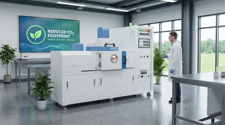
At its core, Chemical Vapor Deposition (CVD) offers a notable environmental benefit by producing a reduced CO2 footprint compared to older, less refined technologies like pitch coating. This advantage stems from the inherent precision and efficiency of the CVD process itself, which minimizes waste and maximizes performance.
The true environmental strength of CVD is not just in what it avoids, but in what it achieves. By enabling the creation of highly precise, durable, and high-performance coatings, CVD promotes resource efficiency, reduces material waste, and extends the functional life of components, leading to a more sustainable outcome.
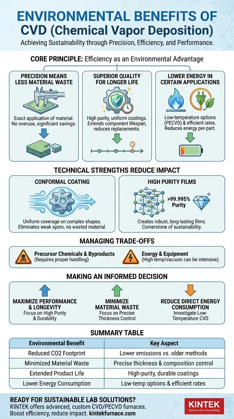
The Principle: Efficiency as an Environmental Advantage
The environmental benefits of CVD are less about a single "green" feature and more a result of its fundamental operational efficiency. The process is designed for precision, which inherently minimizes waste and energy consumption.
Precision Means Less Material Waste
CVD gives engineers exceptional control over the thickness and composition of the deposited film.
This means you apply the exact amount of material needed for the job—no more, no less. This drastic reduction in overuse is a significant source of material savings compared to less precise methods.
Superior Quality for Longer Product Lifecycles
CVD produces coatings of extremely high purity, uniformity, and adhesion.
These superior films protect components from wear, corrosion, and thermal stress far more effectively. By extending the lifespan of the part, CVD reduces the need for frequent replacements, saving the material and energy required to manufacture new ones.
Lower Energy Consumption in Certain Applications
Modern CVD techniques include options for low-temperature deposition.
This allows for coating temperature-sensitive materials without damage and, more importantly, requires significantly less energy than high-temperature processes. Efficient, high deposition rates can also lower the energy consumed per-part.
How CVD's Technical Strengths Reduce Impact
The specific technical characteristics that make CVD a superior coating method are the same ones that contribute to its positive environmental profile.
Conformal Coating: No Weak Spots, No Wasted Material
CVD uses gaseous precursors that can penetrate and uniformly coat highly complex and irregular shapes.
This conformality ensures complete coverage, eliminating weak spots that could lead to premature failure. It also ensures that material is deposited only where it is needed, avoiding the waste associated with line-of-sight techniques that over-coat simple areas to cover complex ones.
High Purity: Creating Robust, Long-Lasting Films
The process is capable of producing films with over 99.995% purity.
Impurities are points of weakness in a coating. By creating an almost perfectly pure layer, CVD delivers exceptional performance and durability, which is a cornerstone of sustainability through longevity.
Process Control: Dialing in the Optimal Footprint
The process parameters in CVD are highly adjustable and repeatable.
This allows operators to optimize the process for both performance and efficiency, minimizing gas flow and energy use while still achieving the desired outcome. This level of control is key to minimizing the operational footprint.
Understanding the Trade-offs
No technology is without its complexities. A balanced assessment of CVD must acknowledge its potential environmental drawbacks.
Precursor Chemicals and Byproducts
CVD relies on precursor gases, some of which can be toxic, flammable, or have a high global warming potential. The process can also create hazardous byproducts.
Proper handling, safety protocols, and exhaust gas abatement systems are absolutely critical to manage these risks and prevent environmental release.
Energy and Equipment Requirements
While low-temperature options exist, many CVD processes still require high temperatures and sophisticated vacuum equipment, which are energy-intensive.
The overall energy balance depends heavily on the specific materials being used and the alternative technology it is being compared against.
Application-Specific Impact
The "green" credentials of CVD are highly context-dependent.
Using a complex CVD process to apply a simple coating that could be done with a low-impact paint is not an environmental win. Its benefits shine in high-performance applications where other methods either fail or are grossly inefficient.
Making an Informed Decision for Your Application
To determine if CVD is the right choice, you must align its strengths with your primary goal.
- If your primary focus is maximizing performance and longevity: CVD's ability to create highly pure and durable coatings is its key advantage, reducing the environmental cost of future replacements.
- If your primary focus is minimizing material waste: The precise thickness control offered by CVD ensures you use the absolute minimum amount of coating material required for your specification.
- If your primary focus is reducing direct energy consumption: Investigate low-temperature CVD variants (like PECVD) that offer significant energy savings over traditional high-temperature thermal processes.
Ultimately, choosing CVD is an investment in precision, quality, and long-term operational efficiency.
Summary Table:
| Environmental Benefit | Key Aspect |
|---|---|
| Reduced CO2 Footprint | Lower emissions vs. older methods like pitch coating |
| Minimized Material Waste | Precise control over film thickness and composition |
| Extended Product Life | High-purity, durable coatings reduce replacement needs |
| Lower Energy Consumption | Options for low-temperature deposition and efficient rates |
Ready to enhance your lab's sustainability with advanced CVD solutions? KINTEK leverages exceptional R&D and in-house manufacturing to provide high-temperature furnaces like CVD/PECVD Systems, Muffle, Tube, Rotary, Vacuum & Atmosphere Furnaces, with deep customization for your unique needs. Contact us today to discuss how our tailored solutions can boost your efficiency and reduce environmental impact!
Visual Guide
Related Products
- Custom Made Versatile CVD Tube Furnace Chemical Vapor Deposition CVD Equipment Machine
- Multi Heating Zones CVD Tube Furnace Machine for Chemical Vapor Deposition Equipment
- HFCVD Machine System Equipment for Drawing Die Nano Diamond Coating
- Split Chamber CVD Tube Furnace with Vacuum Station CVD Machine
- 915MHz MPCVD Diamond Machine Microwave Plasma Chemical Vapor Deposition System Reactor
People Also Ask
- What are the practical applications of gate media prepared by CVD tube furnaces? Unlock Advanced Electronics and More
- How can integrating CVD tube furnaces with other technologies benefit device fabrication? Unlock Advanced Hybrid Processes
- What are the key application fields of CVD tube furnaces? Unlock Precision in Thin-Film Synthesis
- What are the key features of CVD tube furnaces for 2D material processing? Unlock Precision Synthesis for Superior Materials
- How does CVD tube furnace sintering enhance graphene growth? Achieve Superior Crystallinity and High Electron Mobility


