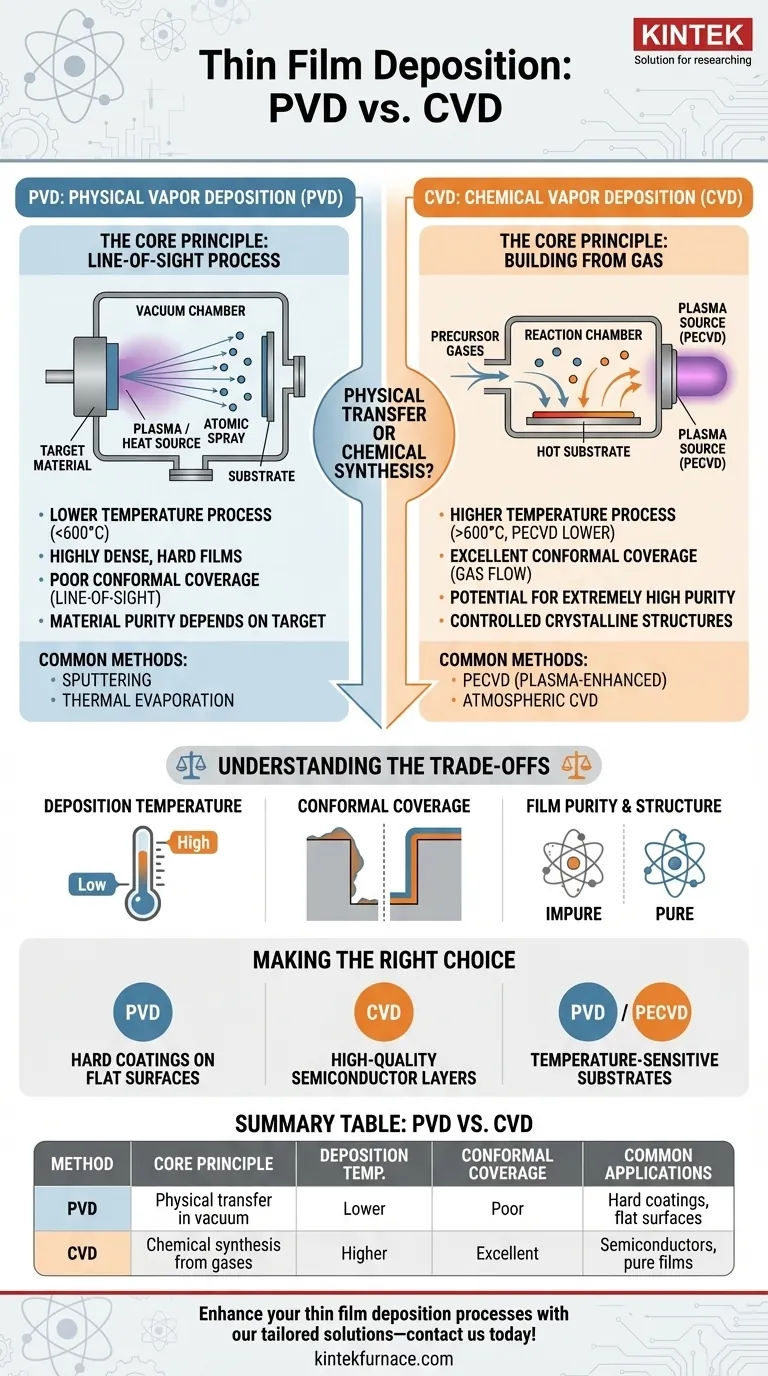
The two dominant methods for creating the ultra-thin layers essential to modern technology are Physical Vapor Deposition (PVD) and Chemical Vapor Deposition (CVD). While both achieve a similar outcome—a thin film on a substrate—they operate on fundamentally different principles. PVD is a physical process that transports material from a source to a substrate, whereas CVD is a chemical process that synthesizes the film directly on the substrate from gaseous precursors.
The choice between PVD and CVD is a foundational decision in materials engineering. It hinges on one key question: is it better to physically move your desired material onto a surface, or to chemically grow it there from scratch?
Understanding Physical Vapor Deposition (PVD)
The Core Principle: A Line-of-Sight Process
PVD operates inside a vacuum chamber by physically ejecting atoms from a solid source material, known as a "target." These ejected atoms travel in a straight line through the vacuum and condense onto the substrate, forming the thin film.
Think of it as a form of atomic spray painting. Because the atoms travel in a straight line, PVD is considered a line-of-sight technique.
Key PVD Characteristics
PVD processes are typically performed at lower temperatures compared to traditional CVD. The resulting films are often very dense and can possess high hardness and wear resistance.
Common PVD methods include sputtering (using an ion plasma to bombard the target) and thermal evaporation (heating the source until it vaporizes).
Deconstructing Chemical Vapor Deposition (CVD)
The Core Principle: Building from Gas
CVD synthesizes a film directly on the substrate through chemical reactions. Precursor gases containing the required chemical elements are introduced into a reaction chamber.
High temperatures or other energy sources cause these gases to react or decompose on the hot substrate surface, leaving behind the desired solid material as a thin film.
The Role of Plasma: Enhancing the Process (PECVD)
A critical variant is Plasma-Enhanced Chemical Vapor Deposition (PECVD). Instead of relying solely on high heat, this method uses an energy source like microwaves to generate a plasma.
This plasma energizes the precursor gases, allowing the chemical reactions to occur at much lower temperatures. This is vital for depositing films on substrates that cannot withstand high heat, such as plastics or certain electronic components.
Understanding the Trade-offs: PVD vs. CVD
Choosing the correct method requires understanding the inherent compromises between the two approaches.
Deposition Temperature
Traditional CVD processes often require very high temperatures (over 600°C) to drive the necessary chemical reactions. This limits the types of substrates that can be used.
PVD and PECVD operate at significantly lower temperatures, making them compatible with a much wider range of materials, including polymers and pre-processed electronic devices.
Conformal Coverage
Conformal coverage refers to the ability of a film to coat complex, three-dimensional topographies uniformly.
Because CVD relies on gases that can flow into and around microscopic features, it provides excellent, highly uniform conformal coatings.
PVD's line-of-sight nature makes it difficult to coat the sides and bottoms of trenches or complex shapes, leading to non-uniform thickness.
Film Purity and Structure
CVD can often produce films with extremely high purity and controlled crystalline structures. Because the film is synthesized atom-by-atom from high-purity gas precursors, it's possible to achieve exceptional material quality.
In PVD, any impurities present in the source target can be transferred directly into the growing film.
Making the Right Choice for Your Application
The selection of PVD versus CVD is driven entirely by the specific requirements of the final product.
- If your primary focus is a hard, dense, metallic, or ceramic coating on a relatively flat surface: PVD is often the more direct, robust, and cost-effective method.
- If your primary focus is an exceptionally pure, uniform, and conformal film for semiconductor manufacturing: CVD is the established industry standard for creating high-quality dielectric and semiconducting layers.
- If your primary focus is coating a temperature-sensitive substrate with a high-quality film: A low-temperature process like PVD or PECVD is essential to prevent damage.
By understanding this fundamental distinction between a physical transfer and a chemical synthesis, you can effectively navigate the landscape of thin film deposition.
Summary Table:
| Method | Core Principle | Deposition Temperature | Conformal Coverage | Common Applications |
|---|---|---|---|---|
| PVD | Physical transfer of material in vacuum | Lower (e.g., < 600°C) | Poor (line-of-sight) | Hard coatings, flat surfaces |
| CVD | Chemical synthesis from gases | Higher (e.g., > 600°C) | Excellent (gas flow) | Semiconductors, pure films |
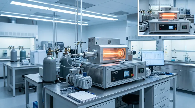
Leveraging exceptional R&D and in-house manufacturing, KINTEK provides diverse laboratories with advanced high-temperature furnace solutions. Our product line, including Muffle, Tube, Rotary Furnaces, Vacuum & Atmosphere Furnaces, and CVD/PECVD Systems, is complemented by our strong deep customization capability to precisely meet unique experimental requirements. Enhance your thin film deposition processes with our tailored solutions—contact us today to discuss how we can support your research and development goals!
Visual Guide
Related Products
- HFCVD Machine System Equipment for Drawing Die Nano Diamond Coating
- RF PECVD System Radio Frequency Plasma Enhanced Chemical Vapor Deposition
- 915MHz MPCVD Diamond Machine Microwave Plasma Chemical Vapor Deposition System Reactor
- MPCVD Machine System Reactor Bell-jar Resonator for Lab and Diamond Growth
- Cylindrical Resonator MPCVD Machine System for Lab Diamond Growth
People Also Ask
- What role does Chemical Vapor Deposition (CVD) equipment play in the surface coating of carbon fibers for composites?
- How can customers maximize the quality of CVD coatings? Master Pre-Coating Prep for Superior Results
- What is the function of high-purity Argon (Ar) gas during CVD? Optimize Your Thin Film Uniformity and Purity
- What core function does CVD equipment serve in h-BN anti-corrosion? Master Precision Synthesis for High-Performance Films
- What materials are commonly used in CVD coating systems? Explore Key Materials for Superior Coatings


