At its core, vapor deposition is a family of processes used to apply very thin, high-performance coatings onto a substrate. The two fundamental techniques are Physical Vapor Deposition (PVD), where a material is physically vaporized and transferred to the substrate, and Chemical Vapor Deposition (CVD), where gases react on the substrate's surface to form the coating.
The choice between PVD and CVD is not about which is "better," but which process mechanics—physical transfer versus chemical reaction—best suit your material, substrate, and desired coating properties like uniformity and heat tolerance.
Understanding Physical Vapor Deposition (PVD)
PVD techniques are fundamentally mechanical at the atomic level. Think of it as dislodging atoms from a source material and having them travel through a vacuum to condense onto your part.
The Core Principle: Physical Transfer
In all PVD processes, the material to be deposited starts as a solid target. Energy is applied to this target in a vacuum chamber, causing atoms or molecules to be ejected.
These vaporized particles travel in a straight line—what's known as line-of-sight deposition—until they strike the substrate and form a thin film.
Common PVD Technique: Sputtering
Sputtering involves bombarding the target material with high-energy ions (typically an inert gas like Argon). This bombardment is like an atomic-scale sandblasting, knocking atoms loose from the target.
These "sputtered" atoms then travel and deposit onto the substrate. Sputtering is highly controllable and creates dense, strongly adhered films, making it ideal for coatings on cutting tools and medical implants.
Common PVD Technique: Evaporation
Evaporation uses heat to melt and then boil the source material, creating a vapor. This can be done by heating the material with a resistive element (thermal evaporation) or by using a high-energy electron beam (e-beam evaporation).
The vapor rises in the vacuum chamber and condenses on the cooler substrate. Evaporation is often faster and simpler than sputtering, used frequently for optical coatings and electronics.
Understanding Chemical Vapor Deposition (CVD)
CVD is a chemical process. Instead of physically transferring a solid material, it introduces specific gases into a chamber that react on a heated surface to create the desired solid film.
The Core Principle: Surface Chemical Reaction
In CVD, one or more volatile gases, known as precursors, are introduced into a reaction chamber. When these gases come into contact with the heated substrate, a chemical reaction is triggered.
This reaction causes a solid material to form and deposit directly onto the substrate surface. Other gaseous byproducts are then pumped out of the chamber.
How CVD Works
The key ingredients for CVD are the precursor gases, energy (usually heat) to drive the reaction, and a controlled environment. Because the coating is formed by a gas that surrounds the part, CVD has a significant advantage.
CVD offers excellent conformality, meaning it can uniformly coat highly complex, non-line-of-sight surfaces and intricate 3D shapes. This is critical for internal surfaces and microelectronics.
Understanding the Trade-offs: PVD vs. CVD
Choosing the right technique requires understanding their fundamental differences in process and outcome.
Operating Temperature
CVD typically requires high temperatures (often >600°C) to energize the chemical reactions. This limits the types of substrates that can be used, as many materials cannot withstand such heat without damage or deformation.
PVD is a lower-temperature process. It can be performed at temperatures from 50°C to 500°C, making it suitable for a much wider range of materials, including heat-sensitive plastics and alloys.
Coating Conformance and Coverage
As a gas-based process, CVD excels at creating highly uniform (conformal) coatings over complex geometries and internal surfaces.
PVD is a line-of-sight process. This can result in thinner coatings on areas not directly facing the source material, requiring complex part rotation to achieve uniformity on 3D objects.
Material Versatility
PVD is extremely versatile and can be used to deposit almost any material that can be made into a solid target, including pure metals, alloys, and many ceramic compounds.
CVD is limited by the availability of suitable precursor chemicals. A stable, volatile precursor gas must exist for the material you wish to deposit, which is not always possible.
Film Purity and Structure
CVD can produce exceptionally pure films with excellent crystalline structure due to the precise chemical nature of the process.
PVD films, while very dense, can sometimes incorporate impurities from the process gas (like Argon in sputtering). However, the process offers fine control over film density and stress.
Making the Right Choice for Your Application
Your specific goal determines the correct deposition technique. Focus on the required properties of the final product.
- If your primary focus is coating complex 3D shapes or internal surfaces: CVD is the superior choice due to its excellent conformality.
- If you are depositing a coating onto a heat-sensitive material: PVD is almost always the correct path due to its lower operating temperatures.
- If you need a hard, wear-resistant coating on a tool or component: PVD techniques like sputtering are the industry standard for their high density and adhesion.
- If your goal is to grow a high-purity, crystalline semiconductor or dielectric film: CVD offers the chemical precision required for advanced electronics.
Ultimately, selecting the right vapor deposition technique is a matter of aligning the process mechanics with your specific material and performance requirements.
Summary Table:
| Feature | Physical Vapor Deposition (PVD) | Chemical Vapor Deposition (CVD) |
|---|---|---|
| Core Principle | Physical transfer of vaporized material | Chemical reaction of gases on a heated surface |
| Operating Temperature | Low (50°C - 500°C) | High (Often >600°C) |
| Coating Uniformity | Line-of-sight; less uniform on complex shapes | Excellent conformality on 3D and internal surfaces |
| Ideal For | Heat-sensitive substrates, hard coatings (tools) | High-purity films, complex geometries (electronics) |
Still Unsure Which Vapor Deposition Technique is Right for Your Project?
At KINTEK, we don't just supply equipment; we provide solutions. Leveraging our exceptional R&D and in-house manufacturing, we offer a comprehensive range of CVD/PECVD Systems and high-temperature furnaces ideal for vapor deposition processes. Our strong deep customization capability allows us to tailor solutions—whether for R&D or production—to precisely meet your unique material and performance requirements.
Let our experts help you select and customize the perfect system for your application.
Contact us today for a personalized consultation!
Visual Guide

Related Products
- RF PECVD System Radio Frequency Plasma Enhanced Chemical Vapor Deposition
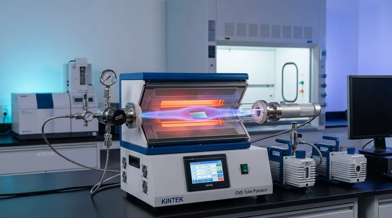
- Custom Made Versatile CVD Tube Furnace Chemical Vapor Deposition CVD Equipment Machine
- MPCVD Machine System Reactor Bell-jar Resonator for Lab and Diamond Growth
- Slide PECVD Tube Furnace with Liquid Gasifier PECVD Machine
- 915MHz MPCVD Diamond Machine Microwave Plasma Chemical Vapor Deposition System Reactor
People Also Ask
- What is PECVD specification? A Guide to Choosing the Right System for Your Lab
- What are the key advantages of PECVD technology? Achieve Low-Temperature, High-Quality Thin Film Deposition
- What is RF in PECVD? A Critical Control for Plasma Deposition
- What are some promising applications of PECVD-prepared 2D materials? Unlock Advanced Sensing and Optoelectronics
- What are the applications of plasma enhanced chemical vapor deposition? Key Uses in Electronics, Optics & Materials


