At its core, chemical vapor deposition (CVD) is a sophisticated manufacturing process that transforms gases into high-performance solid materials. It proceeds through a sequence of steps: reactive gases, known as precursors, are introduced into a controlled chamber, energized by heat, and undergo chemical reactions that cause a solid thin film to form, atom by atom, on a target substrate. The process concludes by cooling the system and purging any leftover gases and byproducts.
The essence of CVD is not merely coating a surface, but orchestrating a precise chemical transformation in a vacuum. It is a method for converting gaseous precursors into a solid, high-purity thin film with atomic-level control.
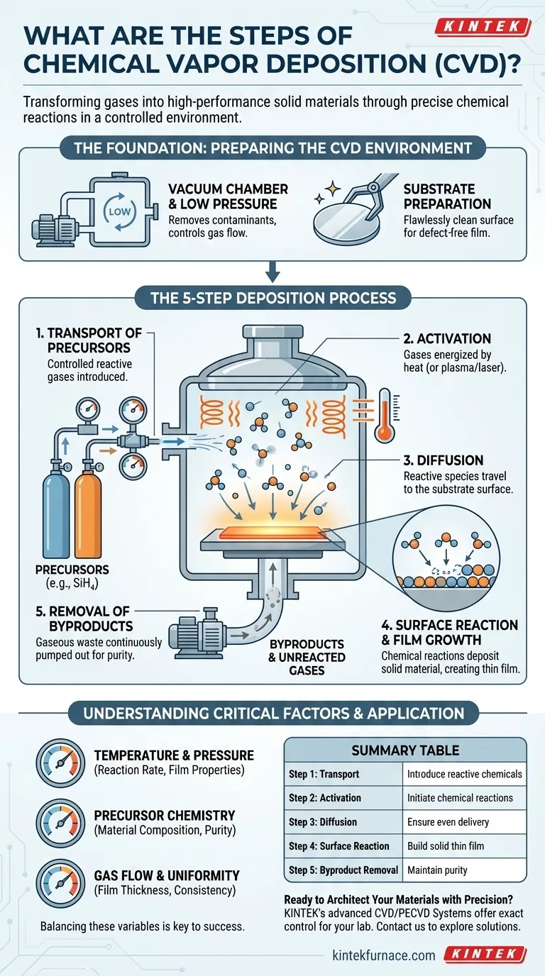
The Foundation: Preparing the CVD Environment
Before any deposition can begin, the system must be meticulously prepared. This stage is critical for ensuring the purity and quality of the final material.
The Role of the Vacuum
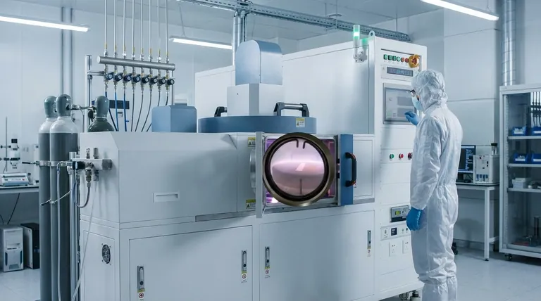
Nearly all CVD processes are performed under vacuum, meaning the pressure inside the reaction chamber is far below normal atmospheric pressure. This serves two vital purposes: removing atmospheric contaminants like oxygen and nitrogen that could cause unwanted reactions, and allowing for precise control over the pressure and flow of the reactive gases.
Preparing the Substrate
The object to be coated, known as the substrate, must be flawlessly clean. Any microscopic dust or residue on its surface will create defects in the film. Substrates undergo rigorous cleaning procedures before being loaded into the chamber to ensure the deposited film adheres properly and is structurally perfect.
A Step-by-Step Breakdown of the Deposition Process
Once the environment is prepared, the core CVD process begins. This can be understood as a five-step sequence that happens continuously within the reactor.
Step 1: Transport of Precursors
Controlled quantities of one or more reactive gases, called precursors, are fed into the reaction chamber. The choice of precursor is critical, as its chemical makeup determines the final material of the thin film (e.g., silane gas, SiH₄, is used to deposit silicon films).
Step 2: Activation of Precursors
The precursor gases must be energized, or "activated," to make them reactive. This is most often accomplished by heating the entire chamber and substrate to very high temperatures (typically hundreds or thousands of degrees Celsius). In other variations, energy is supplied by a plasma or lasers.
Step 3: Diffusion to the Substrate
Once activated, the highly reactive gas molecules and atoms diffuse through the low-pressure environment and travel toward the cooler surface of the substrate. The physics of this gas transport are engineered to ensure an even flow across the entire substrate surface.
Step 4: Surface Reaction and Film Growth
This is the heart of the process. When the activated precursor molecules make contact with the substrate surface, they adsorb (stick to the surface) and undergo chemical reactions. These reactions break the molecules apart, depositing the desired solid material and creating the thin film, one atomic layer at a time.
Step 5: Removal of Byproducts
The chemical reactions that form the solid film also create unwanted gaseous byproducts. These byproducts, along with any unreacted precursor gases, are continuously pumped out of the chamber by the vacuum system. This prevents them from being incorporated into the film as impurities.
Understanding the Trade-offs and Critical Factors
Achieving a perfect film requires balancing several competing factors. The success of a CVD process depends entirely on how well these variables are controlled.
Temperature and Pressure
Temperature is the primary driver of the reaction rate. Higher temperatures generally lead to faster deposition but can also damage sensitive substrates or create unwanted crystal structures. Pressure affects the concentration and flow of precursor gases, directly influencing the uniformity and density of the film.
Choice of Precursor Chemistry
The precursor must be volatile enough to exist as a gas but reactive enough to decompose at the chosen temperature. Its purity is paramount, as any impurities in the source gas can easily become defects in the final film.
Gas Flow and Uniformity
Ensuring that every part of the substrate receives the same concentration of precursor gas is a major engineering challenge. Non-uniform flow leads to a film that is thicker in some areas and thinner in others, which is a critical failure in applications like semiconductor manufacturing.
How to Apply This to Your Project
The specific goals for your material will determine which aspects of the CVD process you need to prioritize.
- If your primary focus is semiconductor manufacturing: You need extreme purity and atomic-level control over film thickness, making precursor purity and precise temperature/pressure control your most critical variables.
- If your primary focus is creating durable protective coatings: Your goal is strong adhesion and a dense film structure, so you should prioritize substrate preparation and process temperatures that promote robust film growth.
- If your primary focus is R&D and material discovery: You need a versatile system with highly flexible control over gas flow, temperature, and pressure to experiment with novel precursor chemistries and deposition conditions.
Ultimately, mastering the steps of chemical vapor deposition allows you to architect materials from the atom up, creating the foundational components for next-generation technology.
Summary Table:
| Step | Key Action | Purpose |
|---|---|---|
| 1. Transport | Precursor gases enter the chamber | Introduce reactive chemicals |
| 2. Activation | Gases are energized (e.g., by heat) | Initiate chemical reactions |
| 3. Diffusion | Activated species move to the substrate | Ensure even delivery to the surface |
| 4. Surface Reaction | Molecules adsorb and react on the substrate | Build the solid thin film, atom by atom |
| 5. Byproduct Removal | Gaseous waste is pumped out | Maintain film purity and quality |
Ready to Architect Your Materials with Precision?
Understanding the steps of CVD is the first step. Implementing them with a furnace that offers exact control over temperature, pressure, and gas flow is what separates a successful project from a failed one.
KINTEK's advanced CVD/PECVD Systems are engineered for this precision. Leveraging our exceptional in-house R&D and manufacturing, we provide the robust, high-temperature platforms necessary to master each stage of the CVD process—ensuring the high-purity, uniform thin films required for semiconductors, protective coatings, and cutting-edge material research.
Let's discuss how our deep customization capabilities can be tailored to your unique experimental requirements.
Contact KINTEK today to explore the right CVD solution for your lab
Visual Guide
Related Products
- Custom Made Versatile CVD Tube Furnace Chemical Vapor Deposition CVD Equipment Machine
- RF PECVD System Radio Frequency Plasma Enhanced Chemical Vapor Deposition
- MPCVD Machine System Reactor Bell-jar Resonator for Lab and Diamond Growth
- Slide PECVD Tube Furnace with Liquid Gasifier PECVD Machine
- 915MHz MPCVD Diamond Machine Microwave Plasma Chemical Vapor Deposition System Reactor
People Also Ask
- How might AI and machine learning enhance CVD tube furnace processes? Boost Quality, Speed, and Safety
- What are the practical applications of gate media prepared by CVD tube furnaces? Unlock Advanced Electronics and More
- What temperature range do standard CVD tube furnaces operate at? Unlock Precision for Your Material Deposition
- What improvements can be made to the bonding force of gate dielectric films using a CVD tube furnace? Enhance Adhesion for Reliable Devices
- How does CVD tube furnace sintering enhance graphene growth? Achieve Superior Crystallinity and High Electron Mobility


