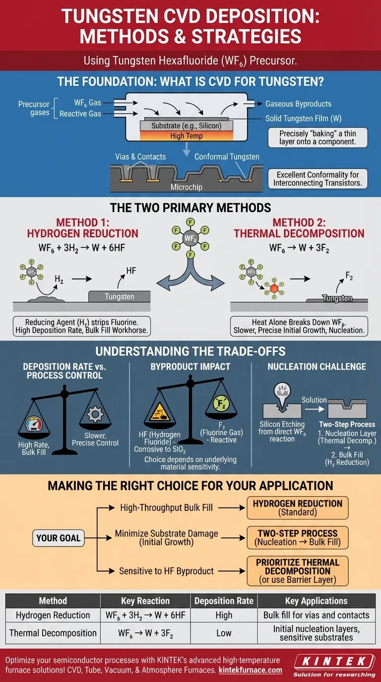
At its core, tungsten deposition via Chemical Vapor Deposition (CVD) is accomplished through two primary methods, both using tungsten hexafluoride (WF₆) gas as the precursor. The first method is hydrogen reduction, where hydrogen gas reacts with WF₆, and the second is thermal decomposition, where heat alone breaks down the WF₆ molecule to deposit pure tungsten.
The choice between these two methods is not arbitrary; it is a strategic decision in semiconductor manufacturing. Hydrogen reduction is the workhorse for high-speed, bulk deposition, while thermal decomposition plays a critical role in the initial, sensitive stages of film growth.
The Foundation: What is Chemical Vapor Deposition?
The Core Principle
Chemical Vapor Deposition (CVD) is a process used to create high-purity solid films on a surface, known as a substrate. Think of it as precisely "baking" a thin layer of material onto a component using reactive gases instead of a liquid batter.
Precursor gases containing the desired atoms are introduced into a reaction chamber. When energy—typically heat—is applied, these gases react on the hot substrate surface, depositing a solid film and leaving behind gaseous byproducts that are then removed.
Why CVD for Tungsten?
In semiconductor manufacturing, millions of transistors on a chip must be interconnected. Tungsten is an excellent conductor used to create these connections, filling tiny vertical channels called vias and forming contacts.
CVD is the ideal method for this task because it provides exceptional conformality. This means it can deposit a uniform tungsten film that perfectly coats the complex, three-dimensional topography of a microchip, ensuring reliable electrical pathways.
The Two Methods for Tungsten CVD Explained
Both primary methods start with tungsten hexafluoride (WF₆) but use different chemical pathways to achieve the final tungsten film.
Method 1: Hydrogen Reduction
This is the most common method for depositing the bulk of a tungsten film. It involves reacting WF₆ with hydrogen (H₂) gas.
The chemical reaction is: WF₆ + 3H₂ → W + 6HF
In this process, hydrogen acts as a reducing agent, chemically stripping the fluorine atoms from the tungsten and forming hydrogen fluoride (HF) gas as a byproduct. This reaction is efficient and offers a high deposition rate.
Method 2: Thermal Decomposition
This method, also known as pyrolysis, relies solely on thermal energy to break down the precursor gas.
The chemical reaction is: WF₆ → W + 3F₂
When heated to a sufficient temperature, the WF₆ molecules become unstable and decompose, depositing solid tungsten (W) and releasing fluorine gas (F₂) as a byproduct. This process is generally slower than hydrogen reduction.
Understanding the Trade-offs
The selection of a deposition method depends on balancing speed, film quality, and the sensitivity of the underlying materials.
Deposition Rate vs. Process Control
Hydrogen reduction is significantly faster, making it the preferred choice for filling large features or depositing thick films where manufacturing throughput is a primary concern.
Thermal decomposition is a slower, often self-limiting process. This slower rate can offer more precise control over the initial few atomic layers of tungsten, which is critical for creating a proper interface.
The Impact of Byproducts
The byproducts of each reaction are a major consideration. The hydrogen fluoride (HF) produced during hydrogen reduction can be corrosive and may etch or damage sensitive underlying materials like silicon oxide.
The fluorine gas (F₂) from thermal decomposition can also be reactive. The choice often depends on which byproduct is less detrimental to the specific layers already present on the substrate.
The Nucleation Challenge
When depositing tungsten directly onto a silicon substrate, the WF₆ can react aggressively with the silicon, etching it and creating defects. To prevent this, a two-step process is often employed.
An initial, thin nucleation layer is deposited using a gentler method (like thermal decomposition or silane reduction) to protect the silicon. Once this foundation is in place, the process switches to the much faster hydrogen reduction to fill the feature.
Making the Right Choice for Your Application
Your goal determines the optimal strategy for tungsten CVD.
- If your primary focus is high-throughput bulk fill for vias and contacts: Hydrogen reduction is the standard industrial method due to its high deposition rate.
- If your primary focus is minimizing substrate damage during the initial film growth: A two-step process is superior, beginning with a gentler nucleation layer before switching to hydrogen reduction for the bulk fill.
- If you are working with materials highly sensitive to hydrogen fluoride (HF): The process chemistry must be carefully tuned, potentially prioritizing a thermal decomposition step or ensuring an effective barrier layer is in place.
Ultimately, mastering tungsten CVD is about leveraging the strengths of both reduction and decomposition to build reliable, high-performance integrated circuits.
Summary Table:
| Method | Key Reaction | Deposition Rate | Key Applications |
|---|---|---|---|
| Hydrogen Reduction | WF₆ + 3H₂ → W + 6HF | High | Bulk fill for vias and contacts |
| Thermal Decomposition | WF₆ → W + 3F₂ | Low | Initial nucleation layers, sensitive substrates |
Optimize your semiconductor processes with KINTEK's advanced high-temperature furnace solutions! Leveraging exceptional R&D and in-house manufacturing, we provide diverse laboratories with tailored CVD systems, including Muffle, Tube, Rotary, Vacuum & Atmosphere Furnaces, and CVD/PECVD Systems. Our strong deep customization capability ensures precise alignment with your unique experimental needs for superior tungsten deposition. Contact us today to enhance your lab's efficiency and achieve reliable, high-performance results!
Visual Guide
Related Products
- Custom Made Versatile CVD Tube Furnace Chemical Vapor Deposition CVD Equipment Machine
- HFCVD Machine System Equipment for Drawing Die Nano Diamond Coating
- Multi Heating Zones CVD Tube Furnace Machine for Chemical Vapor Deposition Equipment
- Inclined Rotary Plasma Enhanced Chemical Deposition PECVD Tube Furnace Machine
- Inclined Rotary Plasma Enhanced Chemical Deposition PECVD Tube Furnace Machine
People Also Ask
- How might AI and machine learning enhance CVD tube furnace processes? Boost Quality, Speed, and Safety
- How does CVD tube furnace sintering enhance graphene growth? Achieve Superior Crystallinity and High Electron Mobility
- What improvements can be made to the bonding force of gate dielectric films using a CVD tube furnace? Enhance Adhesion for Reliable Devices
- What customization options are available for CVD tube furnaces? Tailor Your System for Superior Material Synthesis
- What are the key application fields of CVD tube furnaces? Unlock Precision in Thin-Film Synthesis


