At a fundamental level, thin film deposition processes are categorized into two primary families: Physical Vapor Deposition (PVD) and Chemical Vapor Deposition (CVD). While other methods exist, these two represent the cornerstone technologies used across industries, from semiconductors to aerospace, for applying atom-by-atom layers of material onto a surface.
The critical distinction lies in how the material travels to the surface. PVD is a mechanical process that physically transports atoms, like spray painting. CVD is a chemical process that grows a film from precursor gases reacting on the surface.
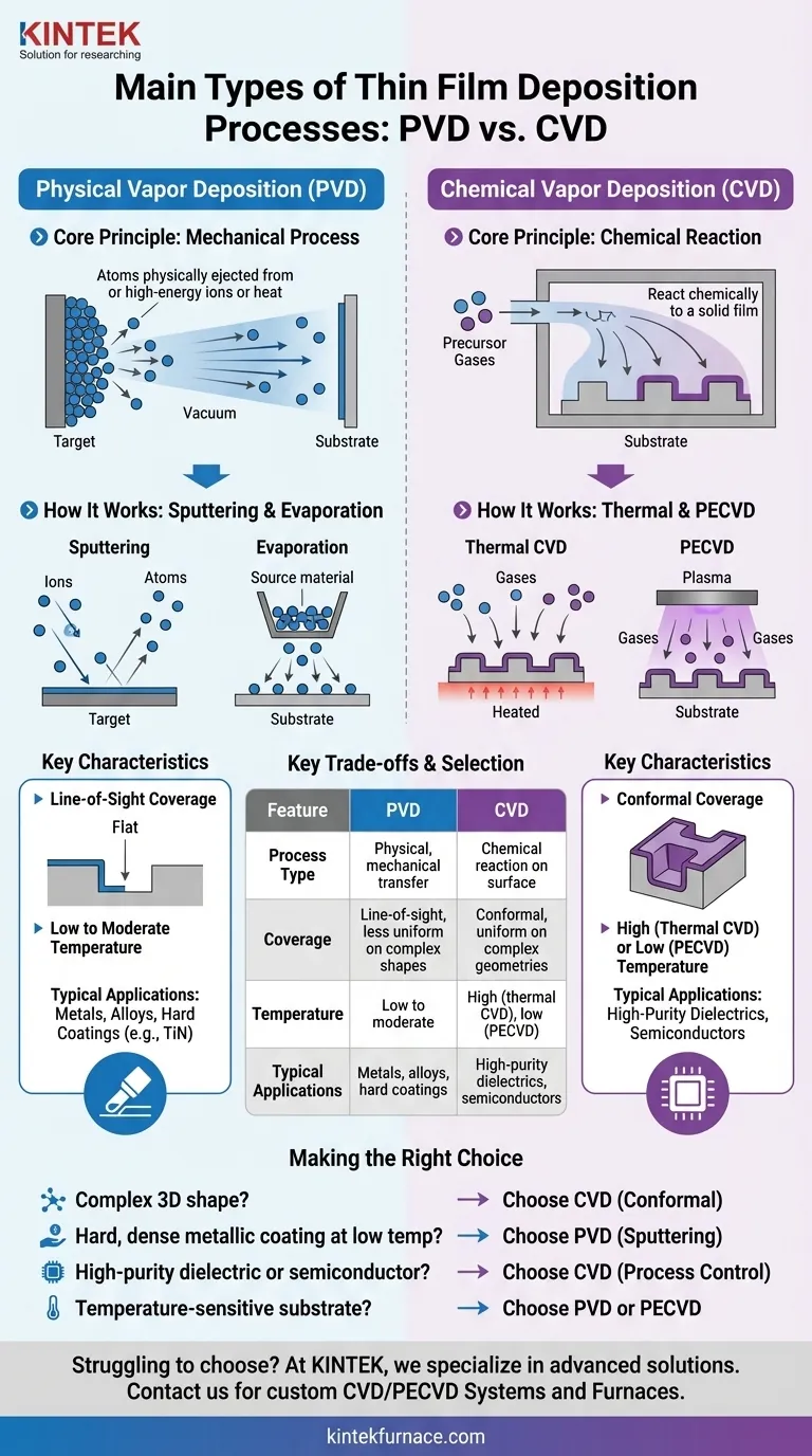
What is Physical Vapor Deposition (PVD)?
Physical Vapor Deposition describes a set of vacuum deposition methods where a material is physically transported from a source to a substrate. It does not involve a chemical reaction to form the film.
The Core Principle: A Mechanical Process
Think of PVD as a highly controlled, atomic-scale spray painting process. Atoms are ejected from a solid source material (called a "target") and travel through a vacuum to land on the substrate, building up the film layer by layer.
How It Works: Sputtering and Evaporation
The two most common PVD methods are sputtering and evaporation.
In sputtering, the target is bombarded with high-energy ions (typically from a gas like argon), which physically knock atoms off its surface. These ejected atoms then deposit onto the substrate.
In thermal evaporation, the source material is heated in a vacuum until it evaporates. The resulting vapor then travels to the cooler substrate, where it condenses to form a solid film.
Key Characteristics of PVD Films
PVD is a line-of-sight process, meaning it coats surfaces that are directly exposed to the source. This makes it less effective for coating complex, three-dimensional shapes with deep trenches or undercuts. It is often performed at relatively low temperatures.
What is Chemical Vapor Deposition (CVD)?
Chemical Vapor Deposition is a process where a substrate is exposed to one or more volatile precursor gases, which react and/or decompose on the substrate surface to produce the desired thin film.
The Core Principle: A Chemical Reaction
Unlike the physical transfer in PVD, CVD grows a film through surface chemistry. Precursor gases are introduced into a reaction chamber, and energy (usually heat) is applied to initiate a chemical reaction that leaves a solid film on the substrate.
Introducing Plasma-Enhanced CVD (PECVD)
A crucial variant is Plasma-Enhanced CVD (PECVD). Instead of relying solely on high temperatures, PECVD uses a plasma to energize the precursor gases. This allows the chemical reaction to occur at much lower temperatures.
Key Characteristics of CVD Films
CVD processes are known for producing highly conformal films, meaning they can coat complex shapes and deep features with excellent uniformity. The resulting films are often very pure and dense, with properties that can be precisely controlled.
Understanding the Key Trade-offs
Choosing between PVD and CVD requires understanding their fundamental differences and the impact on the final product.
Conformal Coverage vs. Line of Sight
CVD excels at conformal coating. Because the precursor gases can diffuse into and react within complex geometries, CVD provides a uniform film thickness over intricate surfaces.
PVD is a line-of-sight technique. It is ideal for coating flat surfaces but struggles to coat shadowed areas, leading to non-uniform thickness on complex parts.
Deposition Temperature
Traditional CVD often requires very high temperatures (several hundred to over 1000°C) to drive the chemical reactions. This can damage temperature-sensitive substrates like plastics or certain electronic components.
PVD and PECVD operate at much lower temperatures. This makes them suitable for a wider range of substrate materials that cannot withstand the heat of thermal CVD.
Material and Film Properties
PVD is a dominant process for depositing metals, alloys, and hard ceramic coatings like titanium nitride (TiN) for wear resistance on cutting tools.
CVD is extremely versatile and is a cornerstone of the semiconductor industry for depositing high-purity silicon, silicon dioxide (a dielectric), and silicon nitride films.
Making the Right Choice for Your Goal
Your application's specific requirements for material, substrate, and film shape will determine the ideal process.
- If your primary focus is coating a complex 3D shape uniformly: Choose CVD for its superior conformal coverage.
- If your primary focus is depositing a hard, dense metallic coating at a low temperature: Choose PVD, specifically sputtering.
- If your primary focus is growing a high-purity dielectric or semiconductor film: Choose CVD for its excellent process control and film quality.
- If your primary focus is coating a temperature-sensitive substrate like a polymer: Choose PVD or Plasma-Enhanced CVD (PECVD) to avoid heat damage.
Ultimately, selecting the right deposition method is a matter of matching the process physics and chemistry to your specific engineering goal.
Summary Table:
| Feature | Physical Vapor Deposition (PVD) | Chemical Vapor Deposition (CVD) |
|---|---|---|
| Process Type | Physical, mechanical transfer | Chemical reaction on surface |
| Common Methods | Sputtering, Evaporation | Thermal CVD, PECVD |
| Coverage | Line-of-sight, less uniform on complex shapes | Conformal, uniform on complex geometries |
| Temperature | Low to moderate | High (thermal CVD), low (PECVD) |
| Typical Applications | Metals, alloys, hard coatings (e.g., TiN) | High-purity dielectrics, semiconductors |
Struggling to choose the right thin film deposition method for your lab? At KINTEK, we specialize in advanced high-temperature furnace solutions tailored to your needs. Leveraging exceptional R&D and in-house manufacturing, our product line—including Muffle, Tube, Rotary Furnaces, Vacuum & Atmosphere Furnaces, and CVD/PECVD Systems—is designed for precision and reliability. With strong deep customization capabilities, we ensure our solutions precisely meet your unique experimental requirements. Enhance your research with equipment that delivers superior performance and durability. Contact us today to discuss how we can support your thin film deposition goals!
Visual Guide
Related Products
- HFCVD Machine System Equipment for Drawing Die Nano Diamond Coating
- RF PECVD System Radio Frequency Plasma Enhanced Chemical Vapor Deposition
People Also Ask
- What are the equipment for chemical vapor deposition? A Guide to the 5 Essential Components
- What core function does CVD equipment serve in h-BN anti-corrosion? Master Precision Synthesis for High-Performance Films
- What is Hot-filament Chemical Vapor Deposition (HFCVD)? Achieve High-Quality Thin Films with Precision Control
- What role does Chemical Vapor Deposition (CVD) equipment play in the surface coating of carbon fibers for composites?
- What is chemical vapor deposition (CVD) and its primary industrial application? Unlock Precision Thin Films for Electronics

