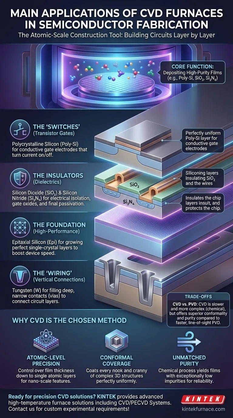
In semiconductor fabrication, the primary application of a CVD furnace is the deposition of ultra-thin, high-purity films on silicon wafers. These films are the fundamental materials used to construct the microscopic components of an integrated circuit. The most common materials deposited include polysilicon (for transistor gates), silicon dioxide (for insulation), and silicon nitride (for protection and insulation).
The true role of a CVD (Chemical Vapor Deposition) furnace is not just to deposit materials, but to act as an atomic-scale construction tool. It enables the precise, uniform layering of conductors, insulators, and semiconductors that form the building blocks of every modern chip.
The Core Function: Building Circuits Layer by Layer
A modern microprocessor is a three-dimensional city of billions of transistors. A CVD furnace is one of the primary tools used to build this city, depositing specific materials in specific locations, layer by atomic layer.
The "Switches": Polycrystalline Silicon (Poly-Si)
Polysilicon is a form of silicon that is conductive enough to act as a gate electrode. This is the "switch" in a transistor that turns the flow of current on and off. CVD is used to deposit a perfectly uniform layer of polysilicon across the wafer.
The Insulators: Silicon Dioxide (SiO₂) and Silicon Nitride (Si₃N₄)
To prevent electrical chaos, components must be electrically isolated from one another. CVD furnaces deposit films of silicon dioxide and silicon nitride, which are excellent electrical insulators (dielectrics).
These films are used to create gate oxides, insulate wires from each other, and form a protective final "passivation" layer over the finished chip to protect it from moisture and contamination.
The Foundation: Epitaxial Silicon (Epi)
For high-performance devices, the process often starts with growing a flawless, single-crystal silicon layer on top of the base wafer. This process, called epitaxial growth, is performed in a CVD furnace and creates a perfect crystal lattice structure, which is essential for optimal electron mobility and device speed.
The "Wiring": Conductive Films
While other methods are often used for metal wiring, CVD is critical for depositing certain conductive films like Tungsten. Its unique ability to "conform" and perfectly fill extremely deep, narrow vertical holes (called contacts or vias) makes it essential for connecting the different layers of the circuit city.
Why CVD is the Chosen Method
Simply depositing a material is not enough; the quality and precision of that deposition are what enable modern electronics. CVD technology provides a level of control that other methods cannot match for these specific applications.
Atomic-Level Precision
Modern transistors have features measured in nanometers. CVD allows for control over film thickness down to the single atomic layer. This precision is non-negotiable for creating consistent, reliable devices across a 300mm wafer.
Conformal Coverage
As transistors have moved to 3D structures (like FinFETs), the surface of a wafer is no longer flat. CVD's key advantage is its conformal coverage—the ability of the deposited film to coat every nook, cranny, and sidewall with a perfectly uniform thickness.
Unmatched Purity and Quality
CVD is a chemical reaction process using high-purity precursor gases. This results in films with exceptionally low levels of impurities, which is critical for achieving the desired electrical properties and long-term reliability of a semiconductor device.
Understanding the Trade-offs
While indispensable, CVD is not the only film deposition technique, and it comes with its own set of challenges.
CVD vs. PVD (Physical Vapor Deposition)
PVD, which includes techniques like sputtering, is a "line-of-sight" physical process. It is often faster and better suited for depositing metal layers for wiring on flatter surfaces.
CVD is a chemical process that is slower but provides the superior conformal coverage and film purity required for dielectrics and complex 3D structures. The two techniques are complementary, not mutually exclusive.
Process Complexity
CVD processes often involve high temperatures and highly toxic, flammable, or corrosive precursor gases. This requires sophisticated safety, handling, and exhaust management systems, adding significant cost and complexity to a fabrication facility.
Throughput and Cost
While large batch furnaces can process hundreds of wafers at once for certain films, more advanced CVD processes require single-wafer processing chambers. This can limit factory throughput and increase the cost per wafer compared to other, faster methods.
Making the Right Choice for Your Goal
The specific CVD application is directly tied to the component being manufactured.
- If your primary focus is building the core transistor: Your key CVD steps are polysilicon for the gate and high-quality silicon dioxide for the gate dielectric.
- If your primary focus is isolating and protecting components: You will rely on CVD to deposit thick layers of silicon nitride and silicon dioxide for insulation and final passivation.
- If your primary focus is creating a high-performance foundation: You will use epitaxial CVD to grow a flawless single-crystal silicon layer on your starting wafer.
- If your primary focus is connecting vertical layers: You will use Tungsten CVD to uniformly fill deep, high-aspect-ratio contacts and vias.
Ultimately, mastering the diverse applications of CVD is fundamental to mastering the art of modern semiconductor manufacturing.
Summary Table:
| Application | Material Deposited | Key Function |
|---|---|---|
| Transistor Gates | Polysilicon | Acts as a conductive switch for current control |
| Insulation | Silicon Dioxide | Provides electrical isolation between components |
| Protection | Silicon Nitride | Shields chips from moisture and contamination |
| Foundation | Epitaxial Silicon | Grows flawless crystal layers for high performance |
| Wiring | Tungsten | Fills vertical holes to connect circuit layers |
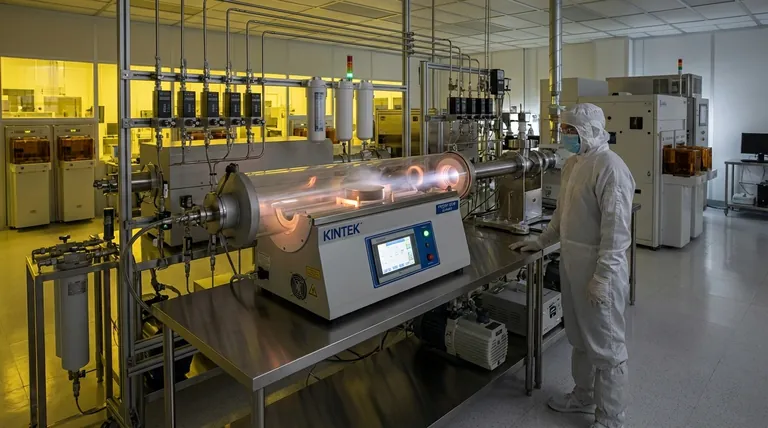
Ready to enhance your semiconductor fabrication with precision CVD solutions? Leveraging exceptional R&D and in-house manufacturing, KINTEK provides diverse laboratories with advanced high-temperature furnace solutions. Our product line, including Muffle, Tube, Rotary Furnaces, Vacuum & Atmosphere Furnaces, and CVD/PECVD Systems, is complemented by our strong deep customization capability to precisely meet unique experimental requirements. Contact us today to discuss how our CVD furnaces can deliver high-purity, conformal films for your semiconductor projects!
Visual Guide
Related Products
- Custom Made Versatile CVD Tube Furnace Chemical Vapor Deposition CVD Equipment Machine
- Split Chamber CVD Tube Furnace with Vacuum Station CVD Machine
- Multi Heating Zones CVD Tube Furnace Machine for Chemical Vapor Deposition Equipment
- Slide PECVD Tube Furnace with Liquid Gasifier PECVD Machine
- Controlled Inert Nitrogen Hydrogen Atmosphere Furnace
People Also Ask
- What are the key features of CVD tube furnaces for 2D material processing? Unlock Precision Synthesis for Superior Materials
- How can integrating CVD tube furnaces with other technologies benefit device fabrication? Unlock Advanced Hybrid Processes
- What future trends are expected in the development of CVD tube furnaces? Discover Smarter, More Versatile Systems
- Why are CVD tube furnace sintering systems indispensable for 2D material research and production? Unlock Atomic-Scale Precision
- Which industries and research fields benefit from CVD tube furnace sintering systems for 2D materials? Unlock Next-Gen Tech Innovations


