At its core, a Chemical Vapor Deposition (CVD) tube furnace is a high-precision tool used to build materials atom by atom. Its primary applications span any field requiring the creation of exceptionally pure, high-performance thin films and coatings, including semiconductor manufacturing, materials science, solar cell production, and the creation of advanced protective coatings.
The true value of a CVD furnace lies not just in what it does, but in the fundamental control it provides. By precisely manipulating precursor gases at high temperatures, it enables the synthesis of materials with specific, engineered properties that are often impossible to achieve through other methods.
Core Application #1: Semiconductor Manufacturing
The semiconductor industry relies on the extreme precision of CVD to build the microscopic structures that power modern electronics.
Fabricating Integrated Circuits
CVD is essential for depositing the ultra-thin, uniform layers of material that form transistors, diodes, and other critical components. This includes depositing materials like silicon, silicon nitride, and the gate media used in advanced MOSFETs.
Growing Crystalline Wafers
The process is also used for the epitaxial growth of materials, creating highly ordered, single-crystal layers on silicon wafers that serve as the foundation for integrated circuits.
Core Application #2: Advanced Materials and Coatings
CVD provides a powerful method for enhancing the properties of existing materials or synthesizing entirely new ones with remarkable characteristics.
Enhancing Industrial Durability
Durable protective layers like titanium nitride (TiN) or silicon carbide (SiC) can be applied to industrial tools, turbine blades, and molds. These hard coatings dramatically improve wear resistance and extend the operational life of the components.
Synthesizing Nanomaterials
CVD is a primary method for synthesizing groundbreaking nanomaterials. This includes the production of high-purity carbon nanotubes, large-area graphene sheets, and synthetic diamond films for a wide range of research and commercial applications.
Core Application #3: Energy and Optics
The ability to create thin films with specific electronic and optical properties makes CVD a cornerstone technology in the energy and display sectors.
Manufacturing Solar Cells
The fabrication of thin-film solar cells depends on CVD to deposit the active photovoltaic layers that convert sunlight into electricity efficiently.
Improving Photoelectric Displays
In the display industry, CVD is used to create the thin-film transistors and emissive layers required for modern LED and OLED screens, enabling brighter and more energy-efficient displays.
Fabricating Optical Components
High-quality coatings are deposited on lenses, mirrors, and optical fibers to control reflectivity, enhance transmission, and protect sensitive surfaces.
Understanding the Trade-offs and Considerations
While powerful, achieving success with CVD requires a deep understanding of its process variables and limitations.
The Critical Role of Precursor Materials
The final material's quality is entirely dependent on the purity and properties of the precursor gases used. A significant area of ongoing research is the development of new precursor materials to unlock novel film properties.
The Need for Precise Process Control
CVD is not a "set it and forget it" technology. Achieving a uniform, defect-free film requires meticulous, real-time control over parameters like temperature, pressure, and gas flow rates, which often involves advanced automation and AI.
Integration with Other Technologies
CVD is often one step in a multi-stage fabrication process. For advanced applications, it may be integrated with other deposition technologies like Atomic Layer Deposition (ALD) or patterning techniques like nanoimprint lithography to create complex, hybrid devices.
Making the Right Choice for Your Goal
To determine if a CVD furnace is the right tool, consider your ultimate objective.
- If your primary focus is high-volume industrial production: Leverage CVD for its proven scalability in applications like semiconductor fabrication, hard coatings for tools, or thin-film solar cells.
- If your primary focus is fundamental research and development: Utilize the furnace's versatility to synthesize novel materials like graphene, test new precursors, or experiment with unique catalytic surfaces.
- If your primary focus is creating highly specialized components: Explore CVD for its precision in fabricating unique parts like wear-resistant biomedical implants or custom-coated optical fibers.
Ultimately, the power of a CVD furnace is its ability to transform simple gases into the advanced materials that define modern technology.
Summary Table:
| Application Field | Key Uses |
|---|---|
| Semiconductor Manufacturing | Fabricating integrated circuits, growing crystalline wafers |
| Advanced Materials and Coatings | Enhancing durability, synthesizing nanomaterials like graphene and carbon nanotubes |
| Energy and Optics | Manufacturing solar cells, improving photoelectric displays, fabricating optical components |
Ready to elevate your lab's capabilities with precision high-temperature solutions? Leveraging exceptional R&D and in-house manufacturing, KINTEK provides diverse laboratories with advanced CVD tube furnaces and other high-temperature systems like Muffle, Tube, Rotary Furnaces, Vacuum & Atmosphere Furnaces, and CVD/PECVD Systems. Our strong deep customization capability ensures we precisely meet your unique experimental requirements, whether for semiconductor production, materials research, or energy applications. Contact us today to discuss how our tailored solutions can drive your innovations forward!
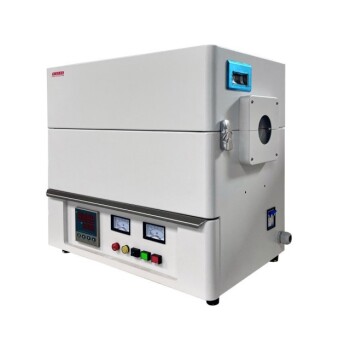
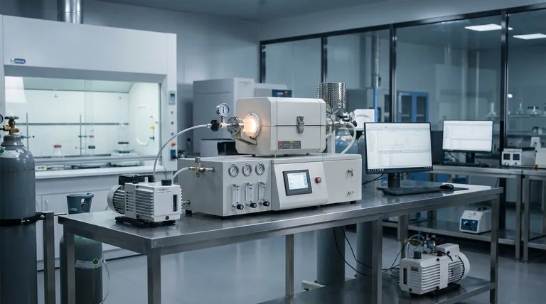
Visual Guide

Related Products
- Custom Made Versatile CVD Tube Furnace Chemical Vapor Deposition CVD Equipment Machine
- Split Chamber CVD Tube Furnace with Vacuum Station CVD Machine
- Multi Heating Zones CVD Tube Furnace Machine for Chemical Vapor Deposition Equipment
- Slide PECVD Tube Furnace with Liquid Gasifier PECVD Machine
- Inclined Rotary Plasma Enhanced Chemical Deposition PECVD Tube Furnace Machine
People Also Ask
- What are the benefits of developing new precursor materials for CVD tube furnaces? Unlock Advanced Thin-Film Synthesis
- What are the practical applications of gate media prepared by CVD tube furnaces? Unlock Advanced Electronics and More
- What temperature range do standard CVD tube furnaces operate at? Unlock Precision for Your Material Deposition
- Why are CVD tube furnace sintering systems indispensable for 2D material research and production? Unlock Atomic-Scale Precision
- What customization options are available for CVD tube furnaces? Tailor Your System for Superior Material Synthesis