At its core, Chemical Vapor Deposition (CVD) technology is valued for its exceptional control, versatility, and efficiency. It is a process that allows for the creation of high-purity, uniform thin films and coatings on a vast array of materials. By carefully managing chemical reactions in a gaseous state, CVD can build materials layer by layer, resulting in superior performance, durability, and functionality across numerous advanced applications.
CVD is not simply a coating method; it is a foundational manufacturing process. Its primary advantage lies in its ability to precisely engineer thin films with specific properties on a wide range of surfaces, enabling the creation of advanced materials central to industries from semiconductors to aerospace.
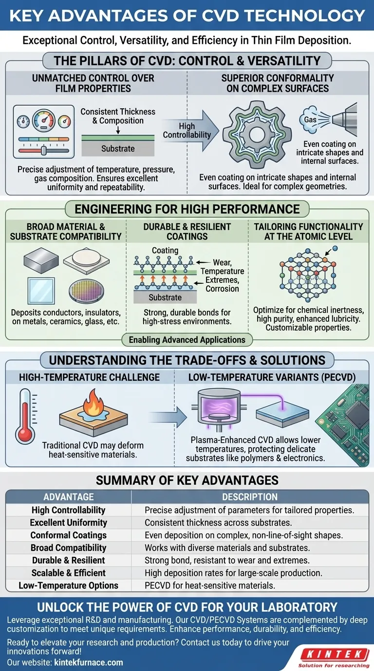
The Pillars of CVD: Control and Versatility
The widespread adoption of CVD stems from its unique ability to combine precision with broad applicability. It offers a level of control that many alternative deposition techniques cannot match.
Unmatched Control Over Film Properties
CVD provides high controllability over the deposition process. By precisely adjusting parameters like temperature, pressure, and gas composition, engineers can dictate the final properties of the film.
This results in excellent uniformity and repeatability. The films produced have a consistent thickness and composition across the entire substrate, ensuring reliable performance from one batch to the next.
Superior Conformality on Complex Surfaces
A key differentiator for CVD is its ability to deposit conformal coatings. The precursor gases can flow around and into complex shapes, coating them evenly.
This makes it ideal for intricate or contoured surfaces, including internal channels and seal areas that are impossible to coat with line-of-sight methods like Physical Vapor Deposition (PVD).
Broad Material and Substrate Compatibility
CVD is incredibly versatile. The process is compatible with a wide variety of precursor gases, allowing for the deposition of everything from insulators to conductors.
Furthermore, these films can be applied to a diverse range of base materials, or substrates, including metals, alloys, ceramics, and glass.
Engineering for High Performance
CVD is used to actively enhance the properties of a material, not just to cover it. The goal is to build a new surface with tailored, superior characteristics.
Creating Durable and Resilient Coatings
CVD creates a strong, durable bond between the coating and the substrate. This ensures the film remains intact even in high-stress, high-wear, or high-vibration environments.
The resulting coatings can also be engineered to withstand extreme temperature variations, making them suitable for demanding aerospace and automotive applications.
Tailoring Functionality at the Atomic Level
The choice of precursor gas allows for the optimization of specific material properties. Coatings can be designed for chemical inertness, corrosion resistance, high purity, or enhanced lubricity.
This ability to tailor coatings is critical for manufacturing advanced semiconductors, efficient solar cells, and durable industrial components.
Enabling Large-Scale and Efficient Production
Compared to many alternatives, CVD is an efficient and cost-effective process. It supports high deposition rates, enabling quick production cycles.
The technology is also scalable, allowing for both large-area deposition on flat panels and selective deposition on pre-patterned substrates, crucial for modern electronics manufacturing.
Understanding the Trade-offs: The Temperature Challenge
No technology is without its limitations. For traditional CVD, the primary consideration is the high operating temperature required to initiate the chemical reactions.
The Drawback of High-Temperature Processes
Standard CVD processes often require very high temperatures, which can be a significant drawback. This heat can cause deformation or structural changes in the substrate material.
For delicate components or materials with low melting points, high-temperature CVD is simply not a viable option, as it can compromise the part's mechanical properties.
The Solution: Low-Temperature Variants
To overcome this limitation, specialized variants have been developed. Plasma-Enhanced CVD (PECVD) is a prime example.
PECVD uses a plasma to energize the precursor gases, allowing the deposition reaction to occur at much lower temperatures. This protects heat-sensitive substrates while still achieving excellent film uniformity and high deposition rates.
The Push for Further Improvement
The main development direction for CVD technology is the continued pursuit of low-temperature and high-vacuum conditions. This research aims to broaden its applicability even further, making its benefits accessible to an ever-wider range of materials and products.
Making the Right Choice for Your Goal
Selecting the appropriate deposition technology depends entirely on your material, budget, and performance requirements. CVD offers a powerful suite of options if its capabilities align with your goals.
- If your primary focus is cost-effective, large-scale production on robust substrates: Traditional high-temperature CVD offers excellent deposition rates and high-purity film quality.
- If your primary focus is depositing films on heat-sensitive materials like polymers or certain electronics: Plasma-Enhanced CVD (PECVD) is the superior choice due to its low-temperature processing capabilities.
- If your primary focus is creating a uniform, pinhole-free coating on complex 3D parts: CVD's inherent conformality gives it a distinct advantage over line-of-sight deposition methods.
By understanding these core principles, you can leverage CVD's unique capabilities to build higher-performing and more durable products.
Summary Table:
| Advantage | Description |
|---|---|
| High Controllability | Precise adjustment of temperature, pressure, and gas composition for tailored film properties. |
| Excellent Uniformity | Consistent thickness and composition across substrates, ensuring reliable performance. |
| Conformal Coatings | Even deposition on complex shapes and internal surfaces, unlike line-of-sight methods. |
| Broad Compatibility | Works with various materials (e.g., metals, ceramics) and substrates for diverse applications. |
| Durable and Resilient | Strong bond and resistance to wear, temperature extremes, and corrosion. |
| Scalable and Efficient | High deposition rates and cost-effectiveness for large-scale production. |
| Low-Temperature Options | Variants like PECVD enable processing of heat-sensitive materials without damage. |
Unlock the Power of CVD for Your Laboratory
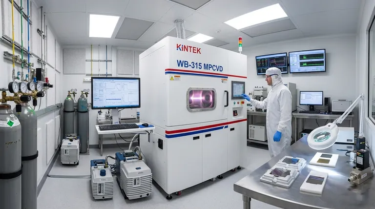
At KINTEK, we leverage exceptional R&D and in-house manufacturing to provide diverse laboratories with advanced high-temperature furnace solutions. Our product line, including Muffle, Tube, Rotary Furnaces, Vacuum & Atmosphere Furnaces, and CVD/PECVD Systems, is complemented by strong deep customization capabilities to precisely meet your unique experimental requirements. Whether you need scalable CVD processes for semiconductors or low-temperature PECVD for delicate materials, we deliver tailored solutions that enhance performance, durability, and efficiency.
Ready to elevate your research and production? Contact us today to discuss how our CVD technologies can drive your innovations forward!
Visual Guide
Related Products
- HFCVD Machine System Equipment for Drawing Die Nano Diamond Coating
- Custom Made Versatile CVD Tube Furnace Chemical Vapor Deposition CVD Equipment Machine
- Cylindrical Resonator MPCVD Machine System for Lab Diamond Growth
- 915MHz MPCVD Diamond Machine Microwave Plasma Chemical Vapor Deposition System Reactor
- MPCVD Machine System Reactor Bell-jar Resonator for Lab and Diamond Growth
People Also Ask
- What is chemical vapor deposition (CVD) and its primary industrial application? Unlock Precision Thin Films for Electronics
- What materials are commonly used in CVD coating systems? Explore Key Materials for Superior Coatings
- What are the equipment for chemical vapor deposition? A Guide to the 5 Essential Components
- What core function does CVD equipment serve in h-BN anti-corrosion? Master Precision Synthesis for High-Performance Films
- What is Hot-filament Chemical Vapor Deposition (HFCVD)? Achieve High-Quality Thin Films with Precision Control


