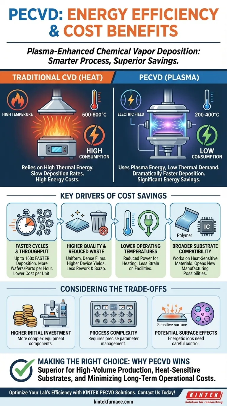
At its core, Plasma-Enhanced Chemical Vapor Deposition (PECVD) delivers significant energy and cost benefits primarily through two mechanisms: operating at much lower temperatures than conventional methods and achieving dramatically faster deposition rates. This combination reduces direct energy consumption while simultaneously increasing manufacturing throughput, leading to substantial savings in operational expenditure.
The fundamental advantage of PECVD is its use of plasma to energize chemical reactions, rather than relying solely on high heat. This decoupling of reaction energy from thermal energy allows for a process that is simultaneously faster, more energy-efficient, and compatible with a wider range of materials.
The Core Principle: Plasma vs. Heat
To understand the cost benefits, you must first understand the fundamental difference between PECVD and traditional Chemical Vapor Deposition (CVD).
Why Traditional CVD is Energy-Intensive
Conventional CVD processes rely on high temperatures, often exceeding 600-800°C, to provide the thermal energy needed to break down precursor gases and drive the chemical reactions for film deposition. Maintaining these high temperatures requires a significant and continuous energy input, making it an inherently expensive process.
How PECVD Reduces Energy Demand
PECVD introduces energy into the system not as heat, but as an electric field that ionizes gases into a plasma. This highly reactive plasma provides the necessary energy to initiate the deposition reactions at much lower temperatures, typically in the 200-400°C range.
This lower operating temperature is the primary driver of PECVD's energy efficiency, directly cutting down on the power required to heat the chamber and substrate.
How Efficiency Translates to Cost Savings
The technical advantages of the PECVD process create several direct and indirect pathways to lower overall costs, especially in production environments.
Increased Throughput and Faster Cycles
The plasma state not only enables lower temperatures but also dramatically accelerates reaction rates. This allows for deposition speeds that can be orders of magnitude faster than traditional CVD.
For example, depositing a material like silicon nitride can be up to 160 times faster with PECVD. This massive increase in throughput means more wafers or parts can be processed in the same amount of time, significantly lowering the cost per unit.
Higher Quality and Reduced Waste
PECVD produces thin films that are highly uniform, dense, and have excellent adhesion with fewer pinholes or cracks. This high quality is a direct result of the energetic but controlled plasma environment.
Higher-quality films lead to higher device yields and less material waste from rejected parts. This reduces the costs associated with rework, scrap, and raw material consumption.
Broader Material and Substrate Compatibility
The low-temperature nature of PECVD makes it possible to deposit films on substrates that cannot withstand high heat, such as polymers or certain integrated circuits.
This versatility opens up new manufacturing possibilities and can be a cost-saver by allowing the use of less expensive or more functional substrate materials that would be damaged by traditional CVD.
Lower Maintenance Overhead
Some PECVD systems are designed for relatively easy chamber cleaning. The process conditions can be less harsh than high-temperature alternatives, potentially leading to less component wear and tear. Reduced downtime for maintenance translates directly to more production time and lower operational costs.
Understanding the Trade-offs
While the operational benefits are clear, PECVD is not without its considerations. A balanced assessment requires acknowledging the trade-offs.
Higher Initial Equipment Cost
PECVD systems are more complex than many conventional CVD reactors. They require sophisticated components like RF power generators, matching networks, and advanced vacuum systems. This typically results in a higher initial capital investment.
Process Complexity
Managing a plasma process involves more variables than a purely thermal one. Parameters like RF power, frequency, pressure, and gas flow must be precisely controlled to achieve desired film properties. This can require a higher level of process engineering expertise.
Potential for Plasma-Induced Damage
While the low temperature is a benefit, the energetic ions within the plasma can sometimes cause damage to the surface of extremely sensitive substrates. This risk must be carefully managed through process tuning, but it remains a consideration for certain advanced applications.
Making the Right Choice for Your Process
Selecting the right deposition technology depends entirely on your specific manufacturing priorities and constraints.
- If your primary focus is high-volume production: PECVD is the superior choice due to its dramatically faster deposition rates, which directly lower the cost per unit.
- If your primary focus is depositing on heat-sensitive substrates: PECVD is often the only viable option, as its low operating temperature prevents damage to materials like plastics or pre-processed semiconductor devices.
- If your primary focus is minimizing long-term operational costs: PECVD's lower energy consumption and higher throughput offer a clear advantage that can quickly offset its higher initial equipment cost.
- If your primary focus is the absolute lowest initial investment: A simpler thermal CVD system might be less expensive upfront, but you must weigh this against its higher long-term energy and production time costs.
Ultimately, PECVD's ability to deliver high-quality films quickly and efficiently makes it the dominant choice for a vast range of modern manufacturing applications.
Summary Table:
| Benefit | Key Impact |
|---|---|
| Lower Operating Temperatures | Reduces energy consumption by 200-400°C vs. 600-800°C in CVD |
| Faster Deposition Rates | Increases throughput, e.g., up to 160x faster for silicon nitride |
| Higher Film Quality | Improves yield and reduces waste with uniform, dense films |
| Broader Substrate Compatibility | Enables use of heat-sensitive materials like polymers |
| Lower Maintenance | Decreases downtime and operational costs with easier cleaning |
Ready to optimize your lab's efficiency with advanced PECVD solutions? KINTEK leverages exceptional R&D and in-house manufacturing to provide high-temperature furnace solutions tailored to your needs. Our product line, including Muffle, Tube, Rotary Furnaces, Vacuum & Atmosphere Furnaces, and CVD/PECVD Systems, is complemented by strong deep customization capabilities to precisely meet unique experimental requirements. Contact us today to discuss how our PECVD systems can deliver energy savings, cost reductions, and enhanced throughput for your laboratory!
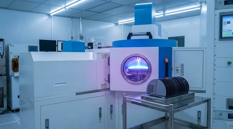
Visual Guide
Related Products
- Slide PECVD Tube Furnace with Liquid Gasifier PECVD Machine
- RF PECVD System Radio Frequency Plasma Enhanced Chemical Vapor Deposition
- Inclined Rotary Plasma Enhanced Chemical Deposition PECVD Tube Furnace Machine
- Inclined Rotary Plasma Enhanced Chemical Deposition PECVD Tube Furnace Machine
- Multi Heating Zones CVD Tube Furnace Machine for Chemical Vapor Deposition Equipment
People Also Ask
- In which industries is the tube furnace commonly used? Essential for Materials Science, Energy, and More
- What are the disadvantages of tube furnace cracking when processing heavy raw materials? Avoid Costly Downtime and Inefficiency
- How does PECVD equipment contribute to TOPCon bottom cells? Mastering Hydrogenation for Maximum Solar Efficiency
- What plasma source is used in PE-CVD tube furnaces? Unlock Low-Temperature, High-Quality Deposition
- How does a hydrogen reduction environment in an industrial tube furnace facilitate gold-copper alloy microspheres?


