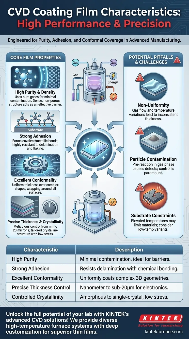
At its core, a coating film produced by Chemical Vapor Deposition (CVD) is known for its high purity, strong adhesion to the substrate, and exceptional ability to conformally coat complex shapes. These films are typically dense, possess good crystallinity, and can be grown with precise thickness control, often in the nanometer to sub-20-micron range.
While CVD is capable of producing exceptionally uniform, high-quality films, this outcome is not automatic. The final characteristics are highly dependent on precise control over process parameters, and a poorly managed process can result in the exact opposite: non-uniform coatings with particle contamination.
Core Film Properties of a Well-Controlled CVD Process
Understanding the ideal characteristics of a CVD film shows why this process is chosen for many advanced manufacturing applications, from semiconductors to aerospace components.
Exceptional Purity and Density
The CVD process uses high-purity precursor gases that react to form the solid film. This method inherently avoids many of the contaminants found in other deposition techniques, resulting in films of very high purity.
These films are also typically dense and non-porous, which is critical for creating effective barrier layers against corrosion or diffusion.
Strong Adhesion
The film is not merely sitting on the surface; it is grown through chemical reactions where the substrate itself often acts as a catalyst. This creates a strong, covalent or metallic bond at the interface between the substrate and the coating.
This chemical integration results in excellent adhesion, making the film highly resistant to delamination or flaking.
Excellent Conformality (Wrap-Around)
One of CVD's most significant advantages is its ability to deposit a film of uniform thickness over complex, three-dimensional surfaces, including trenches, holes, and intricate geometries.
This "wrap-around" capability, known as conformality, is due to the gas-phase nature of the precursors, which can diffuse and reach all exposed surfaces of the substrate before reacting.
Precise Thickness Control
CVD allows for meticulous control over the film's thickness, from a few nanometers up to around 20 microns. This is a stark contrast to traditional methods that deposit much thicker layers (50-500 microns).
This precision is vital for applications in microelectronics and optics, where film thickness directly impacts device performance.
Controlled Crystallinity and Low Stress
By carefully managing process parameters like temperature and pressure, engineers can influence the crystalline structure of the growing film, from amorphous to polycrystalline to single-crystal (epitaxial) layers.
Furthermore, optimized CVD processes can produce films with low residual stress, preventing cracking or warping of the substrate, which is especially important in precision applications.
Understanding the Trade-offs and Potential Pitfalls
The ideal properties of a CVD film are only achieved when the process is perfectly tuned. Understanding the potential failure modes is key to a realistic evaluation.
The Challenge of Uniformity
The most common point of failure is non-uniformity. If gas flow, temperature, or pressure varies across the substrate, the film will grow at different rates, leading to inconsistent thickness.
Achieving high uniformity, especially in large-scale reactors, requires sophisticated engineering to ensure all parts of the substrate experience identical conditions. This is where process control becomes paramount.
Risk of Particle Contamination
If the precursor gases react in the gas phase before reaching the substrate, they can form tiny solid particles. These particles can then fall onto the film, causing defects and contamination.
This issue is mitigated by controlling the temperature and pressure to ensure the chemical reaction occurs primarily on the substrate surface, not in the volume of the reactor.
Substrate and Temperature Constraints
While some variants are considered "low-temperature" processes, many CVD techniques require elevated temperatures to drive the necessary chemical reactions.
This can limit the types of substrate materials that can be coated. For example, standard CVD may be too hot for many polymers or temperature-sensitive electronic components, requiring a specific variant like Plasma-Enhanced CVD (PECVD).
Making the Right Choice for Your Application
Selecting a deposition method depends entirely on the specific requirements of your final product.
- If your primary focus is coating complex 3D shapes or internal surfaces: CVD's exceptional conformality makes it a superior choice over line-of-sight methods like PVD.
- If your primary focus is achieving the highest possible material purity and density: CVD is a leading candidate, especially for semiconductor and optical applications.
- If you are working with heat-sensitive substrates like plastics: You must specifically consider low-temperature variants like Plasma-Enhanced CVD (PECVD) or Atomic Layer Deposition (ALD).
- If your primary focus is rapid, low-cost coating on simple, flat surfaces: The complexity and cost of a high-performance CVD system may be unnecessary, and other methods could be more economical.
Ultimately, CVD provides a powerful toolkit for engineering thin films with precisely controlled properties.
Summary Table:
| Characteristic | Description |
|---|---|
| High Purity | Uses pure precursor gases for minimal contamination, ideal for barrier layers. |
| Strong Adhesion | Forms covalent/metallic bonds, resisting delamination and flaking. |
| Excellent Conformality | Uniformly coats complex 3D shapes like trenches and holes. |
| Precise Thickness Control | Achieves nanometer to sub-20-micron thickness for microelectronics and optics. |
| Controlled Crystallinity | Allows amorphous to single-crystal films with low stress to prevent cracking. |
Unlock the full potential of your lab with KINTEK's advanced CVD solutions! Leveraging exceptional R&D and in-house manufacturing, we provide diverse laboratories with high-temperature furnace systems like CVD/PECVD, Muffle, Tube, Rotary, Vacuum & Atmosphere Furnaces. Our strong deep customization capability ensures precise alignment with your unique experimental needs, delivering superior thin films for semiconductors, aerospace, and more. Contact us today to discuss how we can enhance your research and production processes!
Visual Guide
Related Products
- HFCVD Machine System Equipment for Drawing Die Nano Diamond Coating
- Custom Made Versatile CVD Tube Furnace Chemical Vapor Deposition CVD Equipment Machine
- RF PECVD System Radio Frequency Plasma Enhanced Chemical Vapor Deposition
- Multi Heating Zones CVD Tube Furnace Machine for Chemical Vapor Deposition Equipment
People Also Ask
- What is the function of high-purity Argon (Ar) gas during CVD? Optimize Your Thin Film Uniformity and Purity
- What are the equipment for chemical vapor deposition? A Guide to the 5 Essential Components
- What is chemical vapor deposition (CVD) and its primary industrial application? Unlock Precision Thin Films for Electronics
- What role does Chemical Vapor Deposition (CVD) equipment play in the surface coating of carbon fibers for composites?
- What materials are commonly used in CVD coating systems? Explore Key Materials for Superior Coatings


