In the field of advanced material science, Microwave Plasma Chemical Vapor Deposition (MPCVD) is a leading technique for growing high-quality thin films. Its primary advantages are the ability to produce films with exceptionally high purity and structural uniformity, precise control over material properties, and scalability from research to industrial production.
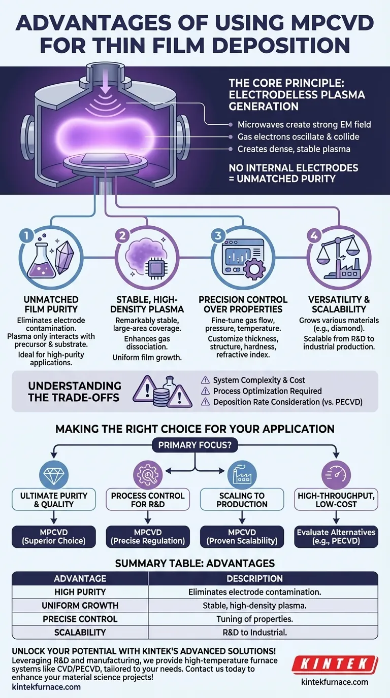
The core advantage of MPCVD isn't just one feature, but how its unique method of plasma generation—using microwaves instead of electrodes—directly leads to films with superior purity and quality. This electrodeless process is the foundation of its most significant benefits.
The Core Principle: Electrodeless Plasma Generation
To understand the advantages of MPCVD, you must first understand how it works. Unlike other plasma-based methods that use internal electrodes, MPCVD generates plasma cleanly and efficiently.
How Microwaves Create Plasma
The process begins by placing a substrate in a vacuum chamber. A precursor gas mixture is introduced, and then microwaves are directed into the chamber.
This microwave energy creates a strong electromagnetic field, causing free electrons in the gas to oscillate and collide with gas molecules. These energetic collisions strip electrons from the molecules, creating a dense, stable plasma without any internal hardware touching it.
The Impact on Film Purity
Because there are no electrodes within the reaction chamber, a major source of contamination is eliminated. In electrode-based systems (like many PECVD setups), the plasma can sputter material from the electrodes, which then gets incorporated into the growing film as impurities. MPCVD completely avoids this issue.
Key Advantages of the MPCVD Process
This unique, electrodeless plasma generation method gives rise to several key operational advantages.
Unmatched Film Purity
The absence of electrode erosion means MPCVD is the go-to method for applications demanding the highest material purity. The plasma only interacts with the precursor gas and the substrate, ensuring the deposited film is free from metallic contamination.
Stable, High-Density Plasma
MPCVD generates a high-density plasma that is remarkably stable and can cover a large area. This stability and density enhance the dissociation of the reactive gas, leading to more efficient and uniform film growth across the entire substrate.
Precision Control Over Material Properties
The process allows for exceptional control over deposition parameters like gas flow, pressure, and temperature. This gives researchers and engineers the ability to precisely tune the final film's properties, such as its thickness, crystalline structure, hardness, and refractive index.
Versatility and Scalability
While famously used for depositing high-quality diamond films, MPCVD is a versatile technique capable of growing a wide range of other materials. Furthermore, the principles are scalable, making it suitable for both small-scale R&D and large-area industrial coating applications.
Understanding the Trade-offs
No technology is without its considerations. To make an objective decision, you must be aware of the potential challenges associated with MPCVD.
System Complexity and Cost
MPCVD systems, with their microwave generators, waveguides, and advanced vacuum chambers, are generally more complex and can have a higher initial capital cost compared to simpler deposition methods.
Process Optimization
While versatile, achieving optimal film quality for a new material requires significant process development. The ideal parameters (gas chemistry, pressure, temperature, power) are highly material-specific and must be carefully tuned.
Deposition Rate Comparison
The deposition rate of MPCVD is highly dependent on the material and process conditions. While efficient for high-quality films like diamond, other methods like PECVD may offer faster deposition rates for certain materials where ultimate purity is less critical.
Making the Right Choice for Your Application
Selecting the right deposition technology depends entirely on your project's primary goal.
- If your primary focus is ultimate material purity and crystalline quality: MPCVD is the superior choice due to its clean, electrodeless plasma generation.
- If your primary focus is process control for sensitive R&D: The precise parameter regulation in MPCVD allows for systematic and repeatable exploration of material properties.
- If your primary focus is scaling a high-quality process to production: MPCVD's proven ability to produce stable, large-area plasma makes it a viable pathway from the lab to the factory.
- If your primary focus is high-throughput, low-cost deposition: It is wise to evaluate MPCVD against alternatives like PECVD, which may offer higher deposition rates for applications where moderate purity is acceptable.
Ultimately, understanding the fundamental process behind MPCVD empowers you to select the right tool for creating superior materials.
Summary Table:
| Advantage | Description |
|---|---|
| High Purity | Eliminates electrode contamination for superior film quality. |
| Uniform Growth | Stable, high-density plasma ensures consistent film deposition. |
| Precise Control | Allows tuning of thickness, structure, and other properties. |
| Scalability | Suitable for both R&D and industrial production applications. |
Unlock the full potential of your thin film deposition with KINTEK's advanced solutions! Leveraging exceptional R&D and in-house manufacturing, we provide diverse laboratories with high-temperature furnace systems like CVD/PECVD, tailored to your unique needs. Our deep customization capabilities ensure precise performance for applications demanding high purity and control. Contact us today to discuss how we can enhance your material science projects!
Visual Guide
Related Products
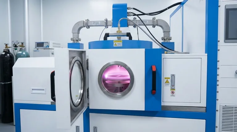
- 915MHz MPCVD Diamond Machine Microwave Plasma Chemical Vapor Deposition System Reactor
- MPCVD Machine System Reactor Bell-jar Resonator for Lab and Diamond Growth
- Cylindrical Resonator MPCVD Machine System for Lab Diamond Growth
- RF PECVD System Radio Frequency Plasma Enhanced Chemical Vapor Deposition
- HFCVD Machine System Equipment for Drawing Die Nano Diamond Coating
People Also Ask
- In which industries is the microwave plasma chemical vapor deposition system commonly used? Unlock High-Purity Material Synthesis
- What is the MPCVD method and why is it considered effective for diamond deposition? Superior Purity & High Growth Rates
- What are the main components of an MPCVD machine? Unlock the Secrets of Diamond Synthesis
- What factors influence the quality of diamond deposition in the MPCVD method? Master the Critical Parameters for High-Quality Diamond Growth
- What are the essential components of an MPCVD reactor system? Build a Pristine Environment for High-Purity Materials


