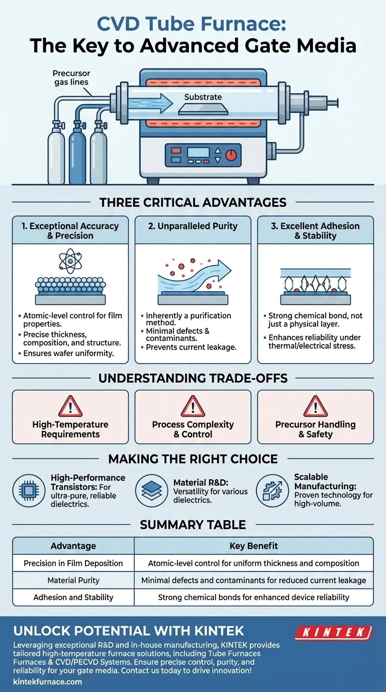
At its core, using a Chemical Vapor Deposition (CVD) tube furnace to prepare gate media provides three critical advantages: exceptional accuracy in controlling film properties, unparalleled purity of the deposited material, and excellent adhesion to the substrate. These attributes are non-negotiable for creating the reliable, high-performance transistors that power modern electronics.
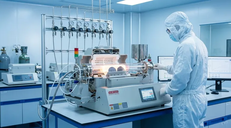
The fundamental challenge in creating a gate dielectric is depositing an atomically precise, ultra-pure, and structurally perfect insulating layer. A CVD tube furnace is the industry-standard tool because it offers the required level of control over the temperature, atmosphere, and chemical reactions necessary to meet these exacting demands.
The Pillars of Gate Dielectric Quality
The gate dielectric is arguably one of the most critical components in a transistor, acting as the insulating barrier that enables the gate to control the flow of current. The quality of this layer directly dictates the device's performance and reliability. A CVD tube furnace provides the ideal environment to perfect it.
Unmatched Precision in Film Deposition
A CVD process allows for atomic-level control over the film's growth. By precisely managing precursor gas flow rates, temperature, and deposition time, you can dictate the exact thickness, chemical composition, and structure of the gate dielectric film.
This precision ensures uniformity across the entire wafer, which is essential for producing millions of identical transistors with consistent performance characteristics.
Achieving Ultimate Material Purity
The CVD process is inherently a purification method. It involves high-temperature chemical reactions where only the desired elements from the precursor gases deposit onto the substrate surface.
Unwanted byproducts and impurities remain in the gas phase and are flushed out of the system. This results in a dielectric layer with minimal defects and contaminants, which is critical for preventing current leakage and ensuring the device's electrical integrity.
Ensuring Strong Adhesion and Stability
CVD creates a strong chemical bond between the deposited film and the underlying substrate, rather than just a physical layer sitting on top.
By optimizing deposition conditions and any subsequent annealing steps, this strong adhesion enhances the overall stability and reliability of the device. This robust interface withstands the thermal and electrical stresses experienced during the transistor's operational life.
Understanding the Trade-offs
While the CVD tube furnace is a powerful tool, it's important to recognize its operational complexities and limitations.
High-Temperature Requirements
Traditional CVD processes often require very high temperatures to drive the necessary chemical reactions. This thermal budget can be a constraint, potentially impacting other temperature-sensitive structures already present on the wafer in later manufacturing stages.
Process Complexity and Control
Achieving the benefits of CVD requires sophisticated equipment. Precise control over gas flows, pressure, and temperature ramps is complex and demands significant process engineering expertise to develop and maintain a stable, repeatable recipe.
Precursor Handling and Safety
The chemicals used as precursors in CVD processes can be highly reactive, toxic, or flammable. Handling these materials requires stringent safety protocols and specialized infrastructure, adding to the operational overhead.
Making the Right Choice for Your Goal
The decision to use a CVD tube furnace is driven by the uncompromising requirements of semiconductor device physics.
- If your primary focus is high-performance transistors: The CVD tube furnace is the definitive choice for creating the ultra-pure, uniform, and structurally sound gate dielectrics needed for reliability and speed.
- If your primary focus is material research and development: The system's versatility allows for experimentation with a wide range of dielectric materials, from standard silicon dioxide and silicon nitride to advanced high-k dielectrics.
- If your primary focus is scalable manufacturing: The CVD process is a proven, mature technology that scales effectively from small-scale laboratory research to high-volume industrial production.
Ultimately, mastering the CVD process within a tube furnace is fundamental to fabricating the advanced gate structures that push the boundaries of semiconductor technology.
Summary Table:
| Advantage | Key Benefit |
|---|---|
| Precision in Film Deposition | Atomic-level control for uniform thickness and composition |
| Material Purity | Minimal defects and contaminants for reduced current leakage |
| Adhesion and Stability | Strong chemical bonds for enhanced device reliability |
Unlock the full potential of your semiconductor processes with KINTEK's advanced CVD tube furnaces. Leveraging exceptional R&D and in-house manufacturing, we provide diverse laboratories with tailored high-temperature furnace solutions. Our product line, including Tube Furnaces, CVD/PECVD Systems, and more, is designed to meet your unique experimental needs with deep customization capabilities. Whether you're developing high-performance transistors or scaling up production, our expertise ensures precise control, purity, and reliability. Contact us today to discuss how we can enhance your gate media preparation and drive innovation in your projects!
Visual Guide
Related Products
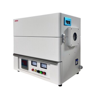
- Custom Made Versatile CVD Tube Furnace Chemical Vapor Deposition CVD Equipment Machine
- Split Chamber CVD Tube Furnace with Vacuum Station CVD Machine
- Multi Heating Zones CVD Tube Furnace Machine for Chemical Vapor Deposition Equipment
- Slide PECVD Tube Furnace with Liquid Gasifier PECVD Machine
- Inclined Rotary Plasma Enhanced Chemical Deposition PECVD Tube Furnace Machine
People Also Ask
- What are the benefits of developing new precursor materials for CVD tube furnaces? Unlock Advanced Thin-Film Synthesis
- Why are CVD tube furnace sintering systems indispensable for 2D material research and production? Unlock Atomic-Scale Precision
- What are the key application fields of CVD tube furnaces? Unlock Precision in Thin-Film Synthesis
- Which industries and research fields benefit from CVD tube furnace sintering systems for 2D materials? Unlock Next-Gen Tech Innovations
- What improvements can be made to the bonding force of gate dielectric films using a CVD tube furnace? Enhance Adhesion for Reliable Devices