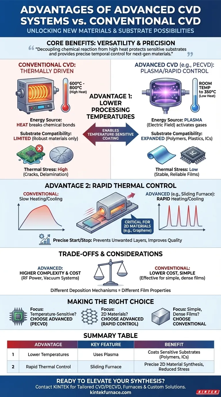
In short, these advanced Chemical Vapor Deposition (CVD) systems offer two primary advantages over conventional methods: they operate at significantly lower temperatures and allow for very rapid heating and cooling. These capabilities are not just minor improvements; they enable the processing of entirely new classes of materials and substrates that are incompatible with traditional high-temperature techniques.
The core benefit is versatility. By decoupling the chemical reaction from high heat, these systems protect sensitive substrates from thermal damage and provide the precise temporal control needed to synthesize complex, next-generation materials like 2D layers.
The Core Advantage: Lower Processing Temperatures
A fundamental limitation of conventional CVD is its reliance on heat. Modern systems, particularly Plasma-Enhanced CVD (PECVD), circumvent this by using an alternative energy source.
The Problem with Conventional CVD
Conventional CVD is a thermally driven process. It uses high temperatures, typically between 600°C and 800°C, to provide the energy needed to break chemical bonds in the precursor gases and deposit a solid film on the substrate.
How Modern Systems Overcome This
Systems like PECVD use an electric field to generate plasma, an ionized gas. This plasma, rather than heat, supplies the energy to activate the precursor gases and drive the deposition reaction.
This crucial difference allows for deposition to occur at much lower substrate temperatures, ranging from room temperature up to 350°C.
The Impact on Substrate Compatibility
The ability to operate at low temperatures dramatically expands the range of usable substrates. Materials that would melt, deform, or be destroyed at 600°C—such as polymers, plastics, or complex integrated circuits—can be coated without damage.
Reducing Thermal Stress and Defects
High temperatures cause materials to expand, and the subsequent cooling causes them to contract. This thermal cycling can create immense stress in thin films, leading to cracks, poor adhesion, or delamination. Lower-temperature processing minimizes this effect, resulting in more stable and reliable films.
The Second Advantage: Rapid Thermal Control
Beyond just a lower operating temperature, some advanced systems offer precise control over the temperature profile itself.
What is Rapid Thermal Cycling?
These systems often incorporate features like a sliding furnace. This mechanical design allows the heat source to be moved over the reaction chamber very quickly, enabling extremely high heating and cooling rates.
Why This Matters for Advanced Materials
This level of control is critical for synthesizing materials where the growth process is highly time-sensitive, such as 2D materials (e.g., graphene or MoS₂).
Rapid heating can initiate the growth phase precisely, while rapid cooling can "quench" the reaction to stop it, preventing the formation of unwanted extra layers. This control over nucleation and growth leads to higher-quality, more uniform materials.
Understanding the Trade-offs
While the advantages are significant, these systems are not a universal replacement for conventional CVD. There are practical considerations to weigh.
System Complexity and Cost
PECVD and other advanced systems are more complex. They require additional equipment like RF power supplies, matching networks, and more sophisticated vacuum systems, which increases their cost and maintenance requirements compared to simpler thermal CVD setups.
Different Film Properties
The deposition mechanism directly influences the final film. Films deposited via PECVD may have different properties—such as hydrogen content, density, or intrinsic stress—than those grown with high-temperature thermal CVD. The ideal process depends entirely on the required characteristics of the final film.
Making the Right Choice for Your Application
Selecting the correct CVD method requires aligning the process capabilities with your primary goal.
- If your primary focus is coating temperature-sensitive substrates: A low-temperature process like PECVD is the only viable option.
- If your primary focus is synthesizing advanced 2D materials: A system with rapid thermal control is essential for achieving the necessary precision.
- If your primary focus is creating simple, dense films on a robust substrate: Conventional thermal CVD remains a cost-effective and highly effective solution.
Ultimately, understanding these advantages empowers you to choose the right tool for the specific material you intend to create.
Summary Table:
| Advantage | Key Feature | Benefit |
|---|---|---|
| Lower Processing Temperatures | Uses plasma instead of heat | Enables coating of temperature-sensitive substrates like polymers and integrated circuits |
| Rapid Thermal Control | Sliding furnace for quick heating/cooling | Allows precise synthesis of 2D materials and reduces thermal stress |
Ready to elevate your material synthesis with advanced CVD solutions? At KINTEK, we leverage exceptional R&D and in-house manufacturing to provide high-temperature furnace solutions tailored to your needs. Our product line includes CVD/PECVD Systems, Muffle, Tube, Rotary Furnaces, and Vacuum & Atmosphere Furnaces, all backed by strong deep customization capabilities to precisely meet your unique experimental requirements. Whether you're working with sensitive substrates or complex 2D materials, we can help you achieve superior results. Contact us today to discuss how our systems can benefit your lab!
Visual Guide
Related Products
- HFCVD Machine System Equipment for Drawing Die Nano Diamond Coating
- Cylindrical Resonator MPCVD Machine System for Lab Diamond Growth
- Custom Made Versatile CVD Tube Furnace Chemical Vapor Deposition CVD Equipment Machine
- 915MHz MPCVD Diamond Machine Microwave Plasma Chemical Vapor Deposition System Reactor
- MPCVD Machine System Reactor Bell-jar Resonator for Lab and Diamond Growth
People Also Ask
- What are the equipment for chemical vapor deposition? A Guide to the 5 Essential Components
- What is Hot-filament Chemical Vapor Deposition (HFCVD)? Achieve High-Quality Thin Films with Precision Control
- What is chemical vapor deposition (CVD) and its primary industrial application? Unlock Precision Thin Films for Electronics
- How can customers maximize the quality of CVD coatings? Master Pre-Coating Prep for Superior Results
- What is the advantage of using a CVD system for coating turbine blades? Master Complex Geometries with Ease