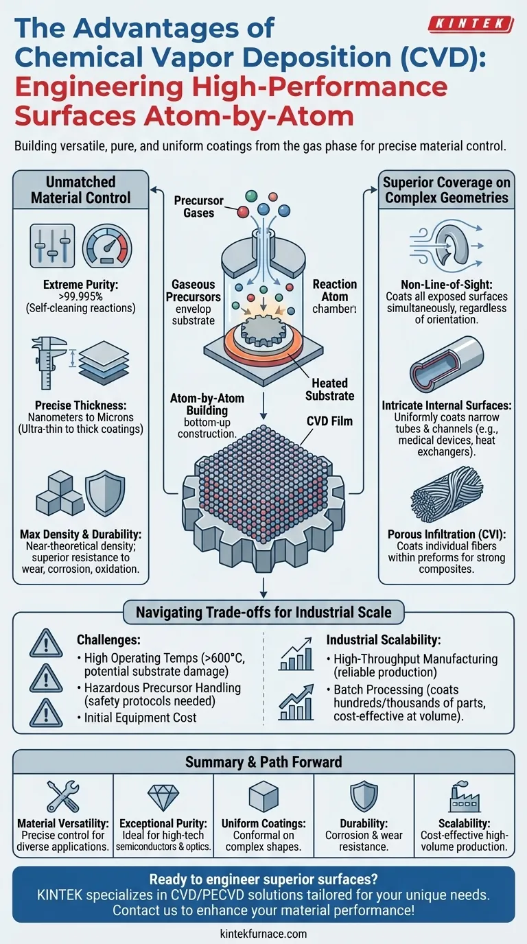
At its core, Chemical Vapor Deposition (CVD) offers a powerful combination of material versatility, exceptional purity, and the unique ability to apply perfectly uniform coatings onto even the most complex surfaces. It is a process that builds high-performance films atom-by-atom from a gas phase, giving engineers precise control over the final material properties.
The true advantage of CVD is not just in applying a coating, but in engineering a new, high-performance surface directly onto a substrate. It transcends simple layering by allowing for the creation of materials with near-perfect purity, density, and uniformity, which is why it is indispensable in high-tech industries.
How CVD Creates Superior Films
To understand its advantages, you must first grasp the process. In CVD, a substrate is placed in a reaction chamber and heated. Precursor gases are then introduced, which react or decompose upon contact with the hot surface, depositing a solid, thin film onto the substrate.
The Role of Gaseous Precursors
The use of a gas is the key. Unlike line-of-sight methods like sputtering, the gas precursors envelop the entire substrate. This fundamental difference is the source of CVD's most significant advantage: conformality.
Building Films Atomically
The deposition occurs as chemical reactions happen on the surface, essentially building the desired material one layer of atoms or molecules at a time. This bottom-up construction gives engineers incredible control over the final product.
Unmatched Control Over Material Properties
CVD is not a blunt instrument; it is a precision tool for materials engineering. This control manifests in the purity, structure, and density of the deposited films.
Achieving Extreme Purity
Because the process uses highly refined precursor gases in a controlled environment, the resulting films are exceptionally pure, often exceeding 99.995% purity. The chemical reactions themselves can have a self-cleaning effect, driving off contaminants.
Engineering Film Thickness and Microstructure
Operators can precisely control film thickness, from a few nanometers to many microns, simply by managing process time, temperature, and gas flow. This allows for the creation of everything from ultra-thin gate dielectrics in a transistor to thick, wear-resistant coatings on industrial tools.
Near-Theoretical Density and Durability
CVD films grow in a way that minimizes voids and defects, resulting in coatings that approach the theoretical maximum density of the material. These dense, well-adhered films are exceptionally durable and provide superior protection against corrosion, oxidation, and wear.
Superior Coverage on Complex Geometries
Perhaps the most defining advantage of CVD is its ability to coat surfaces that are impossible to reach with other methods.
The Power of Non-Line-of-Sight Deposition
Since the precursor gas flows around the entire part, deposition occurs on all exposed surfaces simultaneously, regardless of orientation. This non-line-of-sight capability is a clear differentiator from processes that require a direct path from the source to the substrate.
Coating Intricate Internal Surfaces
This allows CVD to uniformly coat the inside of long, narrow tubes or complex internal channels. This is critical for applications in heat exchangers, fuel cells, and medical devices where internal surface properties are paramount.
Infiltrating Porous Structures
CVD can be used to infiltrate and coat the individual fibers within a fiber preform or a porous foam. This process, known as Chemical Vapor Infiltration (CVI), is used to create strong, lightweight ceramic matrix composites (CMCs) for aerospace applications.
Understanding the Trade-offs
No process is without limitations. Objectivity requires acknowledging where CVD may not be the optimal choice.
High Operating Temperatures
Traditional thermal CVD requires high temperatures (often >600°C) to drive the necessary chemical reactions. This can damage temperature-sensitive substrates, such as plastics or certain metal alloys. However, variants like Plasma-Enhanced CVD (PECVD) operate at lower temperatures to mitigate this.
Precursor Gas Handling
The precursor chemicals used in CVD can be toxic, flammable, or corrosive. This necessitates significant investment in safety protocols, gas handling systems, and abatement equipment, which adds to the operational complexity and cost.
Deposition Rate and Equipment Cost
While some references cite "high deposition rates," this is relative. Compared to processes like thermal spray, CVD can be slower. The vacuum chambers and complex gas delivery systems also represent a significant upfront capital investment.
Economic and Industrial Scalability
Despite the complexities, CVD is a cornerstone of modern manufacturing due to its scalability and cost-effectiveness at volume.
Suitability for High-Throughput Manufacturing
CVD systems are designed for reliable, repeatable production. They can be scaled to coat very large areas, such as architectural glass or large batches of silicon wafers, making the process highly suitable for industrial-scale output.
Batch Processing and Cost-Effectiveness
A single CVD run can process multiple components simultaneously. By coating hundreds or thousands of parts in one batch, the cost per part becomes highly competitive, justifying the initial equipment investment for high-volume applications.
Making the Right Choice for Your Goal
Selecting a deposition technology depends entirely on your primary objective.
- If your primary focus is maximum purity and performance: CVD is the industry standard for creating the ultra-pure, defect-free thin films required in semiconductors and optics.
- If your primary focus is coating complex internal geometries: CVD is often the only viable technology due to its non-line-of-sight deposition capability.
- If your primary focus is durability on a simple shape: You should weigh the superior quality of a CVD coating against the potentially lower cost and higher speed of alternatives like PVD or thermal spray.
- If your primary focus is coating a temperature-sensitive material: You must explore lower-temperature CVD variants like PECVD or consider an alternative process altogether.
Ultimately, CVD empowers you to design the material properties of a surface, not just apply a generic layer to it.
Summary Table:
| Advantage | Key Feature |
|---|---|
| Material Versatility | Precise control over film properties for various applications |
| Exceptional Purity | Films often exceed 99.995% purity, ideal for high-tech uses |
| Uniform Coatings | Conformal deposition on complex shapes, including internal surfaces |
| Durability | Near-theoretical density for corrosion and wear resistance |
| Scalability | Batch processing enables cost-effective high-volume production |
Ready to engineer superior surfaces with advanced CVD solutions? KINTEK specializes in high-temperature furnace systems, including CVD/PECVD, tailored for diverse laboratory needs. Leveraging our strong R&D and in-house manufacturing, we offer deep customization to meet your unique experimental requirements. Contact us today to discuss how our expertise can enhance your material performance and efficiency!
Visual Guide
Related Products
- Custom Made Versatile CVD Tube Furnace Chemical Vapor Deposition CVD Equipment Machine
- MPCVD Machine System Reactor Bell-jar Resonator for Lab and Diamond Growth
- Multi Heating Zones CVD Tube Furnace Machine for Chemical Vapor Deposition Equipment
- 915MHz MPCVD Diamond Machine Microwave Plasma Chemical Vapor Deposition System Reactor
- Slide PECVD Tube Furnace with Liquid Gasifier PECVD Machine
People Also Ask
- Why are CVD tube furnace sintering systems indispensable for 2D material research and production? Unlock Atomic-Scale Precision
- What temperature range do standard CVD tube furnaces operate at? Unlock Precision for Your Material Deposition
- Which industries and research fields benefit from CVD tube furnace sintering systems for 2D materials? Unlock Next-Gen Tech Innovations
- What are the key features of CVD tube furnaces for 2D material processing? Unlock Precision Synthesis for Superior Materials
- How does CVD tube furnace sintering enhance graphene growth? Achieve Superior Crystallinity and High Electron Mobility


