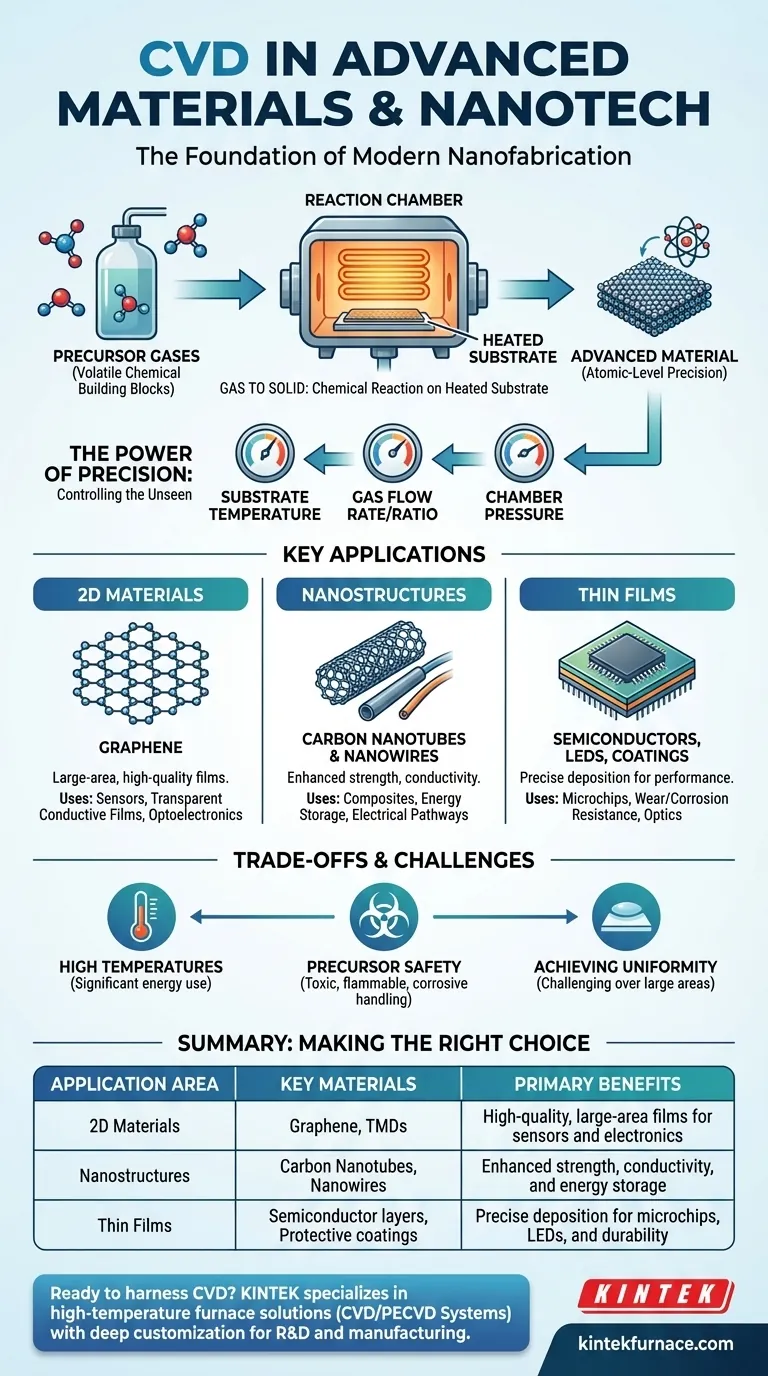
At the heart of modern nanotechnology, Chemical Vapor Deposition (CVD) is the foundational process for fabricating groundbreaking materials. It is applied to grow structures like graphene, carbon nanotubes, and specialized thin films with atomic-level precision, enabling next-generation electronics, optics, and energy solutions.
The true significance of CVD is not just the materials it creates, but its unparalleled ability to control their fundamental properties. By precisely managing a chemical reaction, CVD allows engineers and scientists to dictate a material's thickness, purity, and crystal structure, effectively building advanced materials from the ground up.
The Foundation: How CVD Builds Materials Atom by Atom
At its core, CVD is a deceptively simple concept that enables incredible complexity. It is a process of addition, not subtraction, making it a cornerstone of "bottom-up" nanofabrication.
From Gas to Solid: The Core Principle
CVD works by introducing one or more volatile precursor gases into a reaction chamber. When these gases come into contact with a heated substrate (a base material like a silicon wafer), they react or decompose, depositing a thin, solid film onto the substrate's surface.
The "vapor" in the name refers to the gaseous state of the precursors, which are the chemical building blocks for the final material.
The Power of Precision: Controlling the Unseen
The transformative power of CVD lies in its precise control over the growth environment. By manipulating key parameters, we can directly influence the properties of the deposited material.
Key control variables include the substrate temperature, the flow rate and ratio of precursor gases, and the chamber pressure. This control allows for the creation of materials with specific, desired characteristics, from single-atom-thick layers to complex crystalline structures.
Key Applications in Nanotechnology and Advanced Materials
CVD's precision makes it the go-to method for creating materials whose properties are defined at the nanoscale.
Crafting 2D Materials: Graphene and Beyond
CVD is the leading method for producing large-area, high-quality graphene, a sheet of carbon just one atom thick. This process enables the creation of transparent conductive films, advanced sensors, and next-generation electronic components.
The same principles apply to other 2D materials, such as transition metal dichalcogenides (TMDs), which are critical for innovation in optoelectronics and quantum computing.
Building Nanostructures: Carbon Nanotubes and Nanowires
CVD furnaces are used to grow arrays of carbon nanotubes (CNTs) and nanowires. By controlling catalyst placement and process conditions, engineers can dictate the length, diameter, and density of these structures.
These nanomaterials are used to create high-strength, lightweight composites, highly conductive electrical pathways, and advanced energy storage devices.
Engineering Thin Films for Electronics and Optics
In the semiconductor industry, CVD is an indispensable tool for depositing the multiple thin film layers that make up a microchip. It's also used to create the active layers in LEDs and laser diodes.
Beyond electronics, CVD is used to apply ultra-hard, protective coatings on tools and components, dramatically increasing their resistance to wear and corrosion.
Understanding the Trade-offs and Challenges
While incredibly powerful, CVD is not without its complexities and limitations. Acknowledging these is key to successful implementation.
The Need for High Temperatures
Many CVD processes require very high temperatures, often exceeding 800°C. This high heat consumes significant energy and limits the types of substrates that can be used without melting or degrading.
Precursor Chemistry and Safety
The precursor gases used in CVD can be highly toxic, flammable, or corrosive. Handling these materials requires sophisticated safety systems and protocols, adding complexity and cost to the process.
Achieving Uniformity at Scale
Depositing a perfectly uniform film, especially over large areas like a 300mm silicon wafer, is a major engineering challenge. Slight variations in temperature or gas flow can lead to defects that impact device performance and yield.
Making the Right Choice for Your Goal
The decision to use CVD depends entirely on the material properties you need to achieve.
- If your primary focus is fundamental research on novel materials: CVD offers unmatched control over synthesis, allowing you to explore new material properties with atomic-level precision.
- If your primary focus is scalable electronics manufacturing: CVD is an industry-standard process, but you must invest in systems that can manage uniformity, purity, and throughput to ensure high yield.
- If your primary focus is creating advanced composites or coatings: CVD's ability to grow materials like carbon nanotubes and deposit ultra-hard films provides a distinct performance advantage.
Ultimately, mastering CVD is mastering the art of building functional materials from their most fundamental chemical components.
Summary Table:
| Application Area | Key Materials Produced | Primary Benefits |
|---|---|---|
| 2D Materials | Graphene, TMDs | High-quality, large-area films for sensors and electronics |
| Nanostructures | Carbon Nanotubes, Nanowires | Enhanced strength, conductivity, and energy storage |
| Thin Films | Semiconductor layers, Protective coatings | Precise deposition for microchips, LEDs, and durability |
Ready to harness the power of CVD for your advanced materials projects? KINTEK specializes in high-temperature furnace solutions, including CVD/PECVD Systems, with deep customization to meet your unique experimental needs. Our expertise in R&D and in-house manufacturing ensures precise, reliable results for laboratories in electronics, optics, and energy sectors. Contact us today to discuss how we can elevate your nanotechnology innovations!
Visual Guide
Related Products
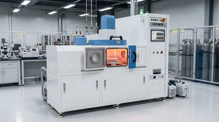
- Custom Made Versatile CVD Tube Furnace Chemical Vapor Deposition CVD Equipment Machine
- Multi Heating Zones CVD Tube Furnace Machine for Chemical Vapor Deposition Equipment
- HFCVD Machine System Equipment for Drawing Die Nano Diamond Coating
- Split Chamber CVD Tube Furnace with Vacuum Station CVD Machine
- 915MHz MPCVD Diamond Machine Microwave Plasma Chemical Vapor Deposition System Reactor
People Also Ask
- Which industries and research fields benefit from CVD tube furnace sintering systems for 2D materials? Unlock Next-Gen Tech Innovations
- What future trends are expected in the development of CVD tube furnaces? Discover Smarter, More Versatile Systems
- What are the benefits of developing new precursor materials for CVD tube furnaces? Unlock Advanced Thin-Film Synthesis
- What is the working principle of a CVD tube furnace? Achieve Precise Thin Film Deposition for Your Lab
- What customization options are available for CVD tube furnaces? Tailor Your System for Superior Material Synthesis


