In essence, the PECVD process uses an energized plasma to break down stable, neutral reactive gas molecules into highly reactive fragments and excited species. These newly active components can then form a solid film on a substrate at much lower temperatures than required by conventional deposition methods.
The core function of plasma in PECVD is to provide the energy for chemical reactions. Instead of relying on high heat, the process uses collisions from high-speed electrons to create reactive chemical precursors, enabling high-quality film deposition on temperature-sensitive materials.
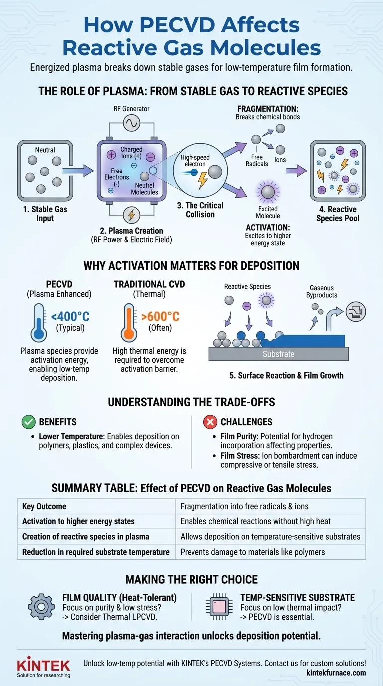
The Role of Plasma: From Stable Gas to Reactive Species
To understand how PECVD works, we must first understand how it generates the building blocks for the film. The process starts with stable gases, which are often unreactive at moderate temperatures.
Creating the Plasma Environment
A low-pressure chamber is filled with the precursor, or "reactive," gas. An electric field, typically generated by a radio frequency (RF) power supply, is then applied across the gas.
This applied energy strips electrons from some gas molecules, creating a mixture of charged ions, free electrons, and neutral gas molecules. This energized, quasi-neutral gas is known as plasma.
The Critical Collision Event
Within the plasma, the free electrons are accelerated to very high speeds by the electric field. These high-speed electrons are the primary drivers of the entire process.
They carry significant kinetic energy and repeatedly collide with the abundant, slower-moving neutral gas molecules that make up the bulk of the chamber's atmosphere.
Fragmentation and Activation
These collisions are highly energetic events that transfer energy directly to the neutral gas molecules. This energy transfer has two main effects:
- Fragmentation: The collision can be powerful enough to break the chemical bonds within the gas molecule, splitting it into smaller, chemically unstable pieces. These fragments are known as free radicals or ions.
- Activation: A less violent collision can excite a molecule into a higher energy state without breaking it apart. This activated molecule is also significantly more reactive than it was in its stable ground state.
The result is a chamber filled with a rich chemistry of ions, electrons, and highly reactive species (radicals and excited molecules) that did not previously exist.
Why This Activation Matters for Deposition
Creating these reactive species is the central purpose of using plasma. It fundamentally changes the conditions required for film growth.
Overcoming the Energy Barrier
All chemical reactions, including the ones that form a solid film, require a certain amount of initial energy to get started, known as activation energy.
In traditional Chemical Vapor Deposition (CVD), this energy is supplied by heating the substrate to very high temperatures (often >600°C). In PECVD, the activation energy is provided by the energetic plasma species, allowing the substrate to remain at a much lower temperature (typically <400°C).
Diffusion and Surface Reaction
Once created, these highly reactive species diffuse from the bulk plasma to the substrate surface. Because they are chemically unstable, they readily bond with the substrate and with each other.
This rapid surface reaction builds the desired solid film layer by layer. Gaseous byproducts from these reactions are continuously removed from the chamber by a vacuum pumping system.
Understanding the Trade-offs
While powerful, the use of plasma introduces specific benefits and challenges that differ from purely thermal processes.
The Key Benefit: Lower Temperature
The primary advantage of PECVD is its ability to deposit films on materials that cannot withstand high heat. This includes polymers, plastics, and complex semiconductor devices with previously fabricated metal layers.
The Challenge: Film Purity and Stress
The energetic and complex nature of the plasma can lead to unintended consequences. For example, hydrogen from precursor gases (like silane, SiH₄) can become incorporated into the deposited film, affecting its electrical and optical properties.
Furthermore, the ion bombardment that occurs during PECVD can induce compressive or tensile stress in the film, which must be carefully managed to prevent cracking or delamination.
Making the Right Choice for Your Goal
Understanding how plasma activates gas molecules allows you to select and tune the right deposition process for your specific objective.
- If your primary focus is film quality on a heat-tolerant substrate: A high-temperature thermal process like LPCVD may yield a purer, lower-stress, and more uniform film.
- If your primary focus is depositing a film on a temperature-sensitive substrate: PECVD is the essential and often only viable choice, as it bypasses the need for high thermal energy.
- If your primary focus is tuning film properties like density or etch rate: You can adjust PECVD parameters like RF power, pressure, and gas chemistry to control the type and energy of the reactive species being created.
Mastering the interaction between plasma and reactive gases is the key to unlocking the full potential of your deposition process.
Summary Table:
| Effect of PECVD on Reactive Gas Molecules | Key Outcome |
|---|---|
| Fragmentation into free radicals and ions | Enables chemical reactions without high heat |
| Activation to higher energy states | Increases reactivity for surface bonding |
| Creation of reactive species in plasma | Allows deposition on temperature-sensitive substrates |
| Reduction in required substrate temperature | Prevents damage to materials like polymers and semiconductors |
Unlock the potential of low-temperature film deposition for your lab with KINTEK! Leveraging exceptional R&D and in-house manufacturing, we provide advanced high-temperature furnace solutions tailored to your needs. Our product line includes Muffle, Tube, Rotary Furnaces, Vacuum & Atmosphere Furnaces, and CVD/PECVD Systems, with strong deep customization capabilities to precisely meet unique experimental requirements. Whether you're working with temperature-sensitive materials or aiming to optimize film properties, our expertise ensures superior performance and reliability. Contact us today to discuss how we can enhance your deposition processes and achieve your research goals!
Visual Guide
Related Products
- Slide PECVD Tube Furnace with Liquid Gasifier PECVD Machine
- RF PECVD System Radio Frequency Plasma Enhanced Chemical Vapor Deposition
- Inclined Rotary Plasma Enhanced Chemical Deposition PECVD Tube Furnace Machine
- Inclined Rotary Plasma Enhanced Chemical Deposition PECVD Tube Furnace Machine
- Multi Heating Zones CVD Tube Furnace Machine for Chemical Vapor Deposition Equipment
People Also Ask
- What role does a Tube Furnace play in the CVD growth of carbon nanotubes? Achieve High-Purity CNT Synthesis
- What are the typical conditions for plasma-enhanced CVD processes? Achieve Low-Temperature Thin Film Deposition
- What are the disadvantages of tube furnace cracking when processing heavy raw materials? Avoid Costly Downtime and Inefficiency
- In which industries is the tube furnace commonly used? Essential for Materials Science, Energy, and More
- What is plasma in the context of PECVD? Unlock Low-Temperature Thin Film Deposition


