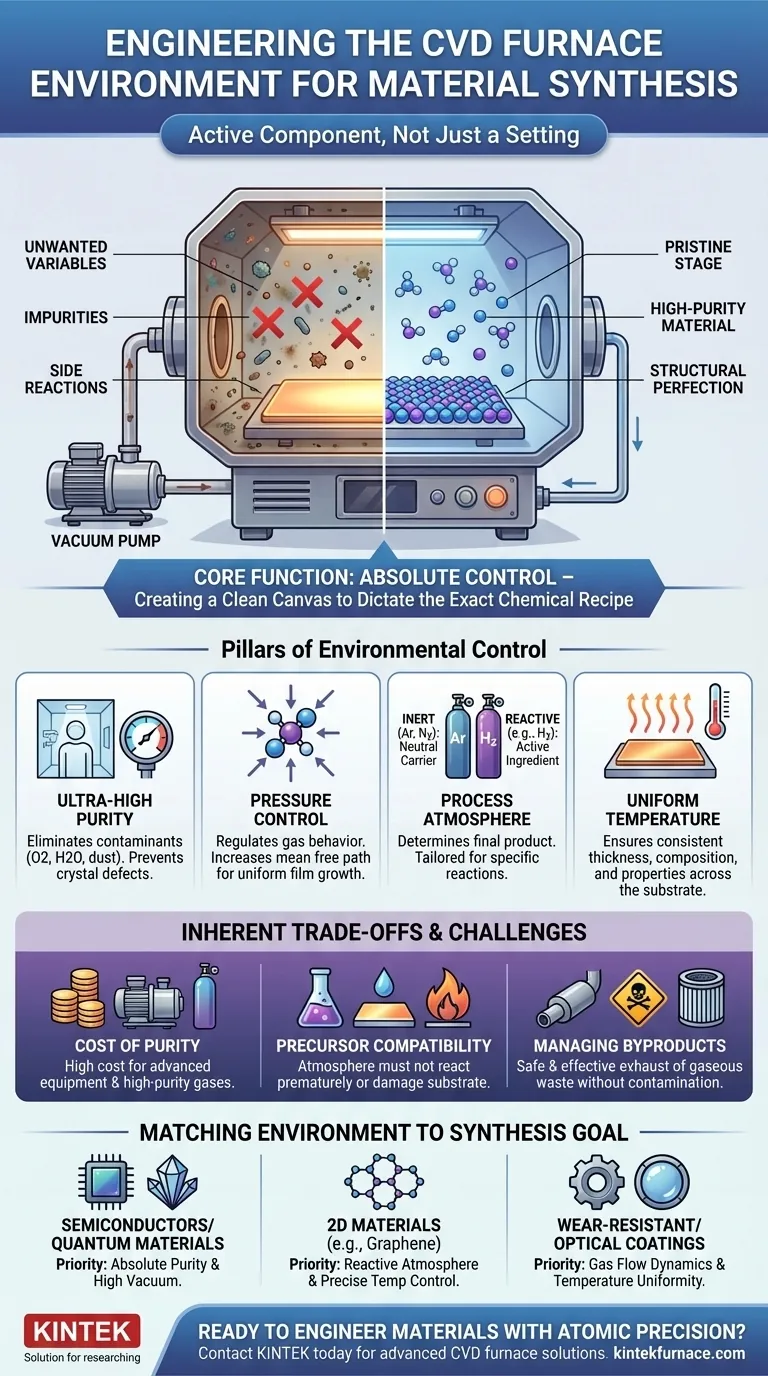
The environment inside a CVD furnace is not just a setting; it is an active, engineered component in material synthesis. The primary contribution of this environment—typically a high vacuum or a precisely controlled atmosphere—is to eliminate all unwanted variables. By removing impurities and preventing side reactions, it creates a pristine stage where only the desired chemical reactions can occur, enabling the creation of high-purity, structurally perfect materials.
The core function of the furnace environment is to provide absolute control. By first creating a clean, empty canvas via vacuum and then introducing specific, high-purity gases, you dictate the exact chemical recipe for the material being grown on the substrate.

The Pillars of Environmental Control in CVD
To understand how this control is achieved, we must look at the key elements that define the furnace's internal environment. Each element serves a distinct purpose in guiding the chemical vapor deposition (CVD) process from raw gases to a solid, high-performance film.
Achieving Ultra-High Purity
The process begins by creating an ultra-pure environment, free from contaminants like oxygen, water vapor, and dust. This is non-negotiable for high-quality synthesis.
Any foreign particle or unwanted gas can act as an impurity, getting trapped in the material's crystal structure. This creates defects that degrade the material's electrical, optical, or mechanical properties.
Think of the furnace as a cleanroom for atoms. Pulling a vacuum is the first step, purging the chamber of ambient air and contaminants.
The Role of Pressure Control
Once purged, the furnace pressure is precisely regulated. This is not simply about maintaining a vacuum; it is about controlling the behavior of the gas molecules.
Low pressure increases the mean free path—the average distance a gas molecule travels before colliding with another. This helps ensure that precursor gases react on the substrate surface rather than in the gas phase, leading to more uniform and higher-quality films.
Selecting the Process Atmosphere
After establishing a clean, low-pressure baseline, specific process gases are introduced. The choice of gas fundamentally determines the final product.
An inert atmosphere, using gases like Argon or Nitrogen, acts as a neutral carrier. These gases transport the reactive precursor gases to the substrate without participating in the chemical reaction.
A reactive atmosphere, in contrast, is an active ingredient. For instance, using a reducing atmosphere (like hydrogen) when heating carbon-containing materials is essential for synthesizing materials like graphene.
Ensuring Uniform Temperature
Finally, the environment must have a highly uniform temperature across the entire substrate. The CVD chemical reactions are extremely sensitive to heat.
If one part of the substrate is hotter than another, the film will grow thicker or with a different structure in that area. Uniform heating ensures the resulting film has consistent thickness, composition, and properties from edge to edge.
Understanding the Inherent Trade-offs
While a controlled environment is powerful, it comes with significant engineering and operational challenges. Acknowledging these trade-offs is crucial for practical application.
The Cost of Purity
Achieving and maintaining an ultra-high purity environment is expensive. It requires sophisticated vacuum pumps, mass flow controllers for precise gas delivery, and the use of high-purity (and costly) process gases.
Precursor and Atmosphere Compatibility
The chemical design of the process is complex. The chosen atmosphere must not react negatively with the precursor gases before they reach the substrate. Likewise, it must not damage the substrate itself at high temperatures.
Managing Reaction Byproducts
The chemical reactions that form the desired film also create gaseous byproducts. These must be safely and effectively exhausted from the chamber without contaminating the process or posing a safety hazard, adding another layer of complexity to the system design.
Matching the Environment to Your Synthesis Goal
The ideal furnace environment is not one-size-fits-all; it must be tailored to the specific material you intend to create.
- If your primary focus is semiconductor films or quantum materials: Your priority is absolute purity and a high-quality vacuum to eliminate crystal defects that would ruin device performance.
- If your primary focus is synthesizing 2D materials like graphene: Your priority is selecting the correct reactive atmosphere (e.g., reducing) and precise temperature control to drive the specific surface chemistry needed.
- If your primary focus is applying wear-resistant or optical coatings: Your priority is often controlling gas flow dynamics and temperature uniformity to ensure consistent film thickness and durability across a large surface area.
By mastering the furnace environment, you move from simply making materials to engineering them with atomic precision.
Summary Table:
| Key Element | Contribution to Material Synthesis |
|---|---|
| Ultra-High Purity | Eliminates contaminants to prevent defects, ensuring high-quality electrical, optical, or mechanical properties. |
| Pressure Control | Regulates gas behavior for uniform film growth by increasing mean free path and reducing gas-phase reactions. |
| Process Atmosphere | Uses inert or reactive gases to transport precursors or drive specific chemical reactions for tailored material outcomes. |
| Uniform Temperature | Ensures consistent film thickness, composition, and properties across the substrate for reliable performance. |
Ready to engineer materials with atomic precision? At KINTEK, we leverage exceptional R&D and in-house manufacturing to provide advanced high-temperature furnace solutions tailored to your needs. Our product line—including Muffle, Tube, Rotary Furnaces, Vacuum & Atmosphere Furnaces, and CVD/PECVD Systems—is complemented by strong deep customization capabilities to precisely meet your unique experimental requirements. Whether you're synthesizing semiconductors, 2D materials, or coatings, our expertise ensures optimal furnace environments for superior results. Contact us today to discuss how we can enhance your material synthesis process!
Visual Guide
Related Products
- Custom Made Versatile CVD Tube Furnace Chemical Vapor Deposition CVD Equipment Machine
- Split Chamber CVD Tube Furnace with Vacuum Station CVD Machine
- Multi Heating Zones CVD Tube Furnace Machine for Chemical Vapor Deposition Equipment
- Slide PECVD Tube Furnace with Liquid Gasifier PECVD Machine
- Inclined Rotary Plasma Enhanced Chemical Deposition PECVD Tube Furnace Machine
People Also Ask
- How might AI and machine learning enhance CVD tube furnace processes? Boost Quality, Speed, and Safety
- Why are CVD tube furnace sintering systems indispensable for 2D material research and production? Unlock Atomic-Scale Precision
- What improvements can be made to the bonding force of gate dielectric films using a CVD tube furnace? Enhance Adhesion for Reliable Devices
- Which industries and research fields benefit from CVD tube furnace sintering systems for 2D materials? Unlock Next-Gen Tech Innovations
- What are the benefits of developing new precursor materials for CVD tube furnaces? Unlock Advanced Thin-Film Synthesis


