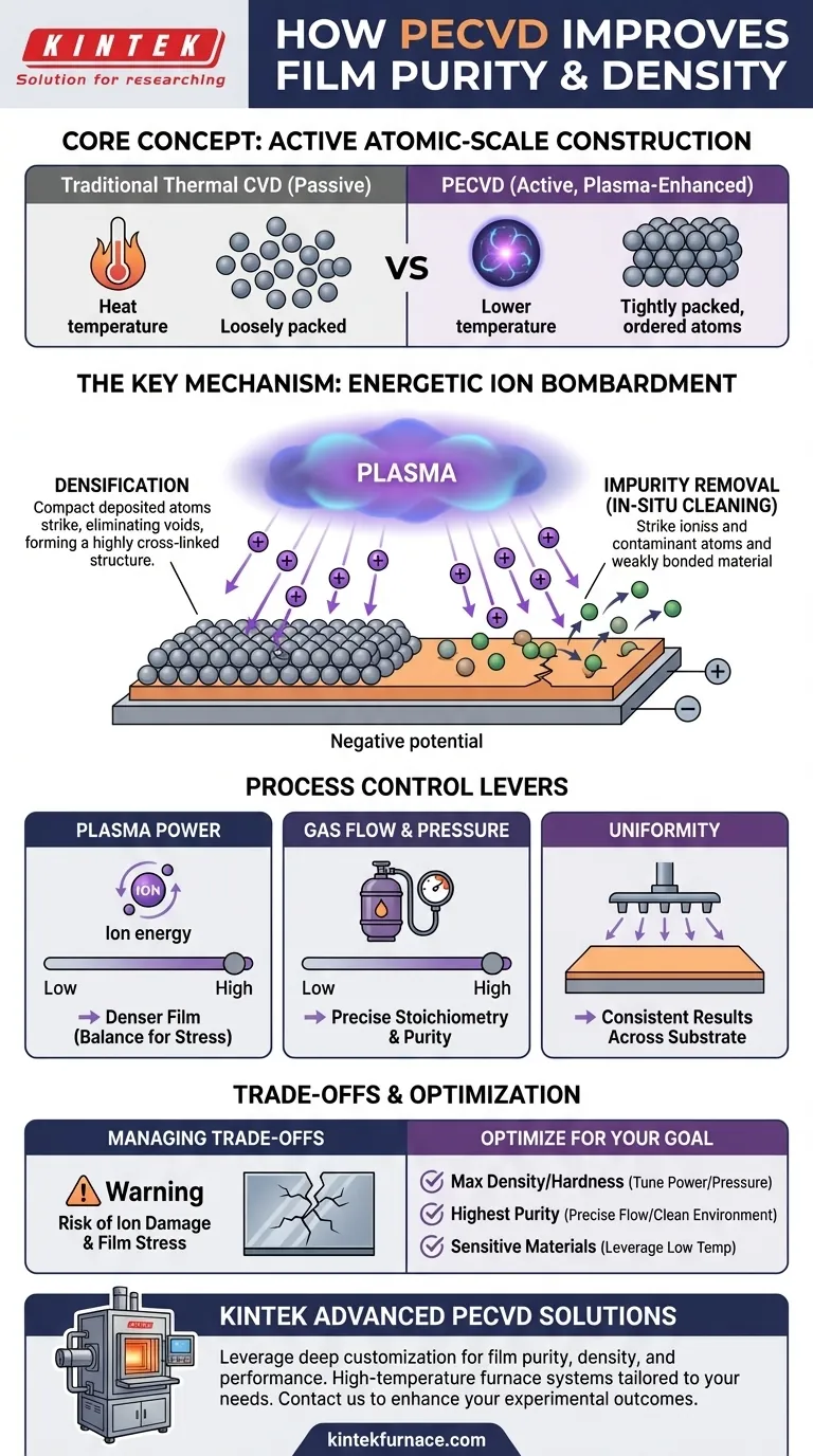
At its core, Plasma-Enhanced Chemical Vapor Deposition (PECVD) improves film purity and density by using an energized plasma to fundamentally change the deposition environment. Unlike purely thermal methods, PECVD creates a flux of energetic ions that actively bombard the growing film, physically compacting the material and sputtering away weakly bonded atoms and contaminants. This dual-action of densification and in-situ cleaning is the primary reason for PECVD's superior film quality at lower temperatures.
The crucial insight is that PECVD is not a passive deposition process. It is an active, atomic-scale construction process where a plasma provides the energy to build denser, purer films without relying on the high temperatures that can damage sensitive substrates.
The Role of Plasma: More Than Just Heat
The defining feature of PECVD is the use of a plasma, an ionized gas containing a mix of ions, electrons, and neutral radical species. This plasma environment is responsible for the unique characteristics of the deposited films.
Creating Reactive Precursors at Low Temperatures
In traditional Chemical Vapor Deposition (CVD), high temperatures are required to break down precursor gases into the reactive species needed for film growth.
The plasma in PECVD accomplishes this with electrical energy instead of thermal energy. It efficiently dissociates the precursor gases at much lower temperatures, creating a high concentration of reactive chemical species.
The Key Mechanism: Energetic Ion Bombardment
The plasma creates a continuous flux of positively charged ions that are accelerated toward the substrate, which is typically held at a negative potential.
These ions strike the surface of the growing film with significant kinetic energy. This physical bombardment acts like a microscopic hammer, compacting the deposited atoms and eliminating voids, which dramatically increases film density. This is also why PECVD films are often described as highly cross-linked.
Sputtering Action for Impurity Removal
The same ion bombardment that increases density also serves as a cleaning mechanism. When an energetic ion strikes the surface, it can transfer enough energy to knock off, or sputter, loosely bonded atoms.
This process preferentially removes contaminants and improperly bonded film material from the surface as it grows. This continuous, in-situ cleaning action is a primary contributor to higher film purity.
How Process Control Translates to Quality
The advantages of PECVD are realized through the precise control of several key process parameters. Each parameter provides a lever to tune the plasma environment and, therefore, the final film properties.
Tuning Plasma Power for Energy Control
The plasma power directly influences the density and energy of the ions striking the film.
Increasing power generally leads to more energetic ion bombardment, resulting in a denser film. However, this must be carefully balanced, as excessive power can induce stress or damage.
Managing Gas Flow and Chamber Pressure
The gas flow rates determine the chemical composition of the plasma and the availability of precursor species for deposition. Chamber pressure affects the mean free path of particles and the energy of the ions.
Controlling these parameters is critical for achieving the correct film stoichiometry and minimizing the incorporation of unwanted elements, thus ensuring purity.
The Importance of Uniformity
Modern PECVD systems are engineered for highly uniform gas distribution and stable temperature profiles across the entire substrate.
This uniformity ensures that every part of the substrate experiences the same plasma conditions, resulting in a film with consistent density, purity, and thickness from edge to edge.
Understanding the Trade-offs
While powerful, the mechanisms in PECVD are not without their complexities and potential downsides. True mastery of the process involves managing these trade-offs.
The Risk of Ion-Induced Damage
The very ion bombardment that densifies the film can also cause damage if not properly controlled. Excessively energetic ions can create defects within the film structure or even damage the underlying substrate, which is a major concern in sensitive semiconductor applications.
Film Stress as a Byproduct
The constant "hammering" from ion bombardment can induce significant compressive stress in the film. While sometimes desirable, this internal stress can cause film cracking, delamination, or warping of the substrate if not managed.
Parameter Interdependence
The process parameters in PECVD are highly interdependent. Adjusting plasma power to increase density will also affect the deposition rate and potentially the film's chemical composition. Achieving a desired outcome requires a holistic understanding of how these variables interact.
Making the Right Choice for Your Application
Applying PECVD successfully means aligning its capabilities with your primary goal. The process offers a wide tuning range to optimize for different film properties.
- If your primary focus is maximum density and hardness: Prioritize the optimization of plasma power and pressure to achieve controlled, energetic ion bombardment without inducing excessive stress.
- If your primary focus is highest purity and stoichiometry: Concentrate on precise gas flow control and maintaining a clean chamber environment, using moderate ion energy to assist with surface cleaning.
- If your primary focus is deposition on sensitive materials: Leverage PECVD's key advantage of low substrate temperatures, which is made possible by the plasma's energy, to deposit high-quality films without damaging the substrate.
Ultimately, PECVD empowers you to engineer the properties of a thin film at an atomic level through the controlled application of plasma energy.
Summary Table:
| Key Aspect | Impact on Film Purity and Density |
|---|---|
| Energetic Ion Bombardment | Compacts atoms and eliminates voids, increasing density; sputters contaminants, improving purity |
| Plasma Power Control | Adjusts ion energy for denser films; must balance to avoid stress or damage |
| Gas Flow and Pressure Management | Ensures stoichiometry and minimizes impurities for higher purity |
| Uniformity in Systems | Provides consistent plasma conditions for uniform density and purity across substrates |
| Low-Temperature Operation | Enables high-quality deposition on sensitive materials without thermal damage |
Elevate your laboratory's capabilities with KINTEK's advanced PECVD solutions! Leveraging exceptional R&D and in-house manufacturing, we provide diverse laboratories with high-temperature furnace systems, including CVD/PECVD Systems, tailored to your unique needs. Our strong deep customization capability ensures precise optimization for film purity, density, and performance. Contact us today to discuss how our expertise can enhance your experimental outcomes and drive innovation in your projects!
Visual Guide
Related Products
- Slide PECVD Tube Furnace with Liquid Gasifier PECVD Machine
- RF PECVD System Radio Frequency Plasma Enhanced Chemical Vapor Deposition
- Inclined Rotary Plasma Enhanced Chemical Deposition PECVD Tube Furnace Machine
- Inclined Rotary Plasma Enhanced Chemical Deposition PECVD Tube Furnace Machine
- Multi Heating Zones CVD Tube Furnace Machine for Chemical Vapor Deposition Equipment
People Also Ask
- In which industries is the tube furnace commonly used? Essential for Materials Science, Energy, and More
- How does a hydrogen reduction environment in an industrial tube furnace facilitate gold-copper alloy microspheres?
- How does PECVD equipment contribute to TOPCon bottom cells? Mastering Hydrogenation for Maximum Solar Efficiency
- What are the disadvantages of tube furnace cracking when processing heavy raw materials? Avoid Costly Downtime and Inefficiency
- What is plasma in the context of PECVD? Unlock Low-Temperature Thin Film Deposition


