The direct result of annealing silicon-rich oxide (SiOx) at 1000°C in nitrogen is a profound structural densification and optical transformation. This high-temperature process collapses the film's porous structure, driving out defects and causing a significant reduction in thickness. Simultaneously, the thermal energy forces a phase separation, where excess silicon atoms precipitate into elemental nanocrystals embedded within a newly formed, stoichiometric silicon dioxide matrix, fundamentally altering the material’s refractive index, absorption, and light-emitting properties.
The deep need driving this question is likely understanding how to controllably engineer a composite film of silicon nanocrystals in a SiO2 matrix. The 1000°C nitrogen anneal doesn't just fix defects; it provides the precise thermodynamic conditions to nucleate luminescent nanocrystals while simultaneously stabilizing the insulating matrix, a process that requires balancing densification stress against the desired optical functionality.
The Fundamental Structural Transformation
The 1000°C treatment is not a simple drying out of the film. It is an energetic reconstruction of the entire material system. An as-deposited SiOx film is a metastable, disordered network of silicon and oxygen atoms. High-temperature annealing provides the activation energy needed to reorganize into a dramatically more stable and technologically useful, two-phase composite.
Densification and Severe Thickness Collapse
The most immediate structural effect is a massive contraction of the film volume. The thermal energy drives out structural voids, unbound species, and vacancies, causing the matrix to compact.
This thickness reduction is not uniform; it scales directly with the concentration of excess silicon. While a standard sub-stoichiometric film might shrink by only 6%, a highly silicon-rich composition can experience a dramatic thickness collapse of up to 25%. This extreme shrinkage generates intense transient stress, particularly constrained by the rigid substrate, which must be managed by controlled heating to prevent film rupture.
Surface Smoothing and Interface Priming
Atomic-scale reordering during annealing directly impacts the film's surface topology. As measured by Atomic Force Microscopy (AFM), the high-temperature process drives a reduction in surface roughness.
This smoothing is a direct result of minimizing surface energy. The migration of atoms at 1000°C eliminates nanoscale peaks and valleys, creating a flatter, more controlled interface. For device integration—such as in non-volatile memory or optical emitters—this atomically smooth surface is critical for reliable electrical contact and minimizing light scattering.
Internal Phase Separation and Matrix Conversion
The most critical structural event is happening inside the film. The thermal energy overcomes the kinetic barriers preventing the non-stoichiometric SiOx from achieving thermodynamic stability. This triggers a phase separation into pure silicon clusters and near-stoichiometric SiO2.
The silicon sub-oxide matrix (e.g., SiO1.74) acts as both a source material and a host. Annealing converts the matrix into fully oxidized, insulating SiO2, restoring broken silicon-oxygen bonds. Simultaneously, the excess silicon atoms that were previously randomly dispersed are expelled, diffuse, and nucleate into ultrasmall silicon nanocrystals (nc-Si). A highly porous film—which may start with a porosity of ~62%—can be consolidated down to ~47% as the structure reorganizes.
Optical Property Modulation Through Heating
These structural rearrangements aren’t just physical; they completely redefine how the film interacts with light. The conversion from a homogeneous, amorphous silicon sub-oxide to a heterogeneous SiO2-Si nanocrystal composite allows for "fine-tuning" of optical performance.
Shifting Refractive Index and Absorption
Before annealing, the film's refractive index (n) and extinction coefficient (k) are dictated by a random mix of Si-O bonds and excess silicon. After phase separation, these constants become a function of the volume fraction of high-index silicon nanocrystals embedded in the low-index silica.
This structural change gives researchers a lever to control the optical band gap. By varying the initial silicon excess (and thus the resulting nanocrystal size and density), the absorption edge and dispersion characteristics can be systematically engineered, transforming a lossy, undefined layer into a precisely defined optical medium.
Enabling Light Emission via Quantum Confinement
The ultimate goal of this process is often to engineer luminescence. The amorphous, as-deposited SiOx film is a poor light emitter due to its high defect density, which provides non-radiative recombination pathways.
Annealing at 1000°C creates a scenario where light emission becomes possible. The newly formed silicon nanocrystals (nc-Si) act as quantum dots. When their size is smaller than the Bohr exciton radius of silicon, quantum confinement widens the band gap, allowing for room-temperature photoluminescence. The surrounding SiO2 matrix passivates the nanocrystal surface, further boosting emission efficiency by trapping charge carriers in the active core.
Understanding the Risks and Critical Requirements
The path to achieving these properties is narrow and fraught with potential failure modes that are intrinsic to high-temperature processing.
Managing the Sintering-Dewetting Trade-off
This is the central process challenge. To achieve full densification and phase separation, the film must be heated to a temperature where atomic mobility is high. However, this same condition also triggers constrained sintering failure mechanisms.
The differential shrinkage between the film and the rigid substrate creates enormous tensile stress. This stress can drive grain boundary grooving, pinhole expansion, and Rayleigh instabilities, ultimately causing the thin film to break up into isolated islands and uncover the substrate. To prevent this, the heating schedule must be designed to rapidly complete densification before these strain-driven morphological instabilities can disrupt the continuous coating structure.
Avoiding Unwanted Oxidation and Defects
The inert nitrogen atmosphere is non-negotiable but represents a point of hidden contamination risk. Any trace of oxygen or water vapor in the furnace environment at 1000°C will aggressively oxidize the exposed silicon, counteracting the controlled internal phase separation and altering the final stoichiometry in an uncontrolled way.
A high-precision furnace with a controlled ramp rate and strict gas-tight environment is therefore essential. The process is exceptionally sensitive to temperature uniformity; any cold spot leads to incomplete phase separation, while a hot spot could trigger dewetting. The furnace is not just a heater but the primary instrument for ensuring the repeatable dielectric properties and optical uniformity of the final film.
Making the Right Choice for Your Goal
The decision to use a 1000°C nitrogen anneal depends entirely on your target application and the initial properties of your SiOx film, and it necessitates rigorous process control.
- If your primary focus is creating luminescent silicon quantum dots: This process is the gold standard. Your critical parameter is balancing the initial stoichiometry to control final nanocrystal size, which directly dictates the emission wavelength.
- If your primary focus is creating robust, low-defect coatings: You must manage the sintering stress. Prioritize a slow, multi-stage heating ramp to the target temperature to allow the film to densify without cracking or dewetting from the substrate.
- If your primary focus is using the film as an active optical layer: The change in refractive index (n) and extinction coefficient (k) is your primary design tool. Use the relationship between annealing parameters and phase separation to fine-tune these optical constants for specific waveguide or anti-reflective requirements.
The journey from a disordered, porous SiOx film to a highly functional composite of silicon nanocrystals in a silica matrix is ultimately a furnace-defined sequence of stress management and thermodynamic phase selection.
Summary Table:
| Process Aspect | Pre-Annealing (As-Deposited) | Post-1000°C N2 Annealing | Key Material Effect |
|---|---|---|---|
| Film Structure & Density | Metastable, porous, disordered sub-oxide network | High densification; up to 25% thickness reduction | Eliminates voids and drives structural compaction |
| Phase Composition | Homogeneous Si sub-oxide (e.g., SiO1.74) | Pure Si nanocrystals (nc-Si) in SiO2 matrix | Thermally driven thermodynamic phase separation |
| Surface Morphology | Higher nanoscale roughness | Atomically smoother surface | Minimizes surface energy; enhances device contacts |
| Optical Behavior | High defect density; non-luminescent | Tunable band gap, refractive index & room-temp PL | Quantum confinement in nc-Si enables light emission |
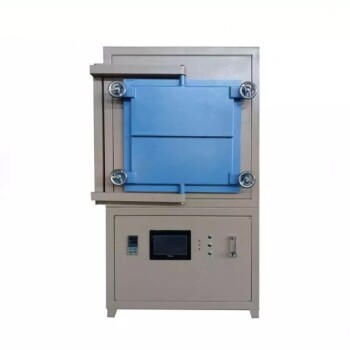
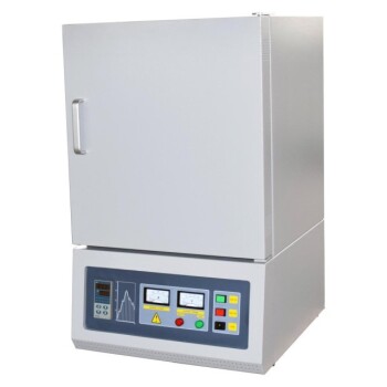
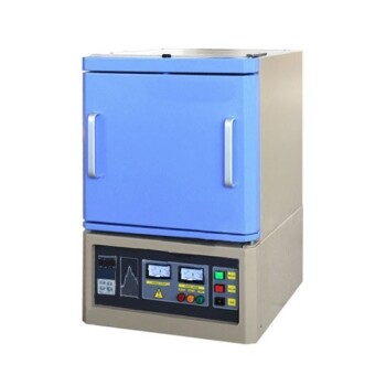
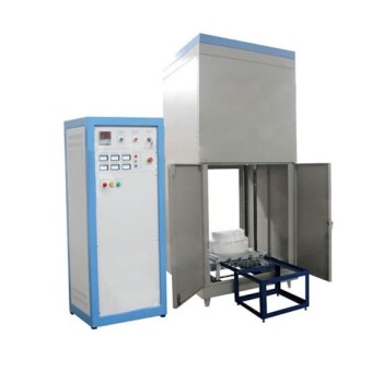
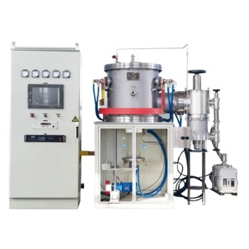
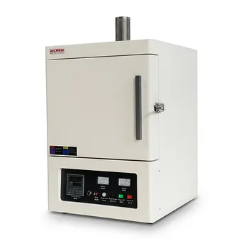
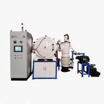
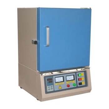
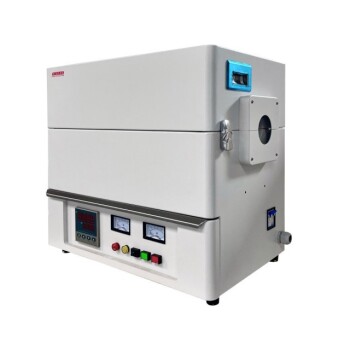
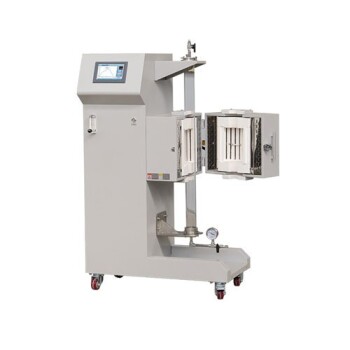
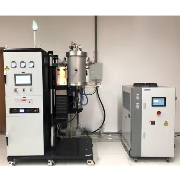
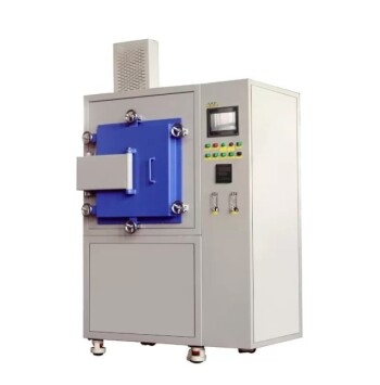
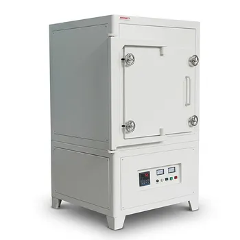
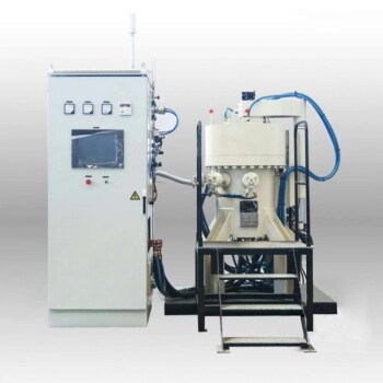
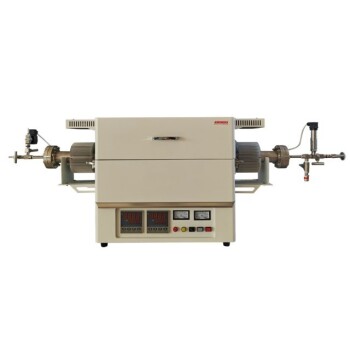
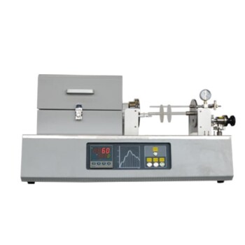
Achieving precise phase separation while avoiding film dewetting during 1000°C thermal processing requires uncompromising atmospheric purity and exact ramp rate control. At KINTEK, we specialize in premium laboratory equipment and consumables, offering a complete range of customizable high-temperature furnaces—including atmosphere, tube, vacuum, CVD, and muffle furnaces—engineered to meet the strict demands of semiconductor and thin-film research. Ensure repeatable optical performance and crack-free film densification for your laboratory—contact KINTEK today to consult with our high-temperature equipment experts!
Related Products
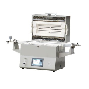
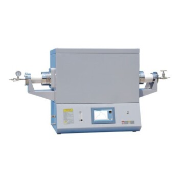
- 1400℃ High Temperature Laboratory Tube Furnace with Alumina Tube
- 1700℃ High Temperature Laboratory Tube Furnace with Alumina Tube
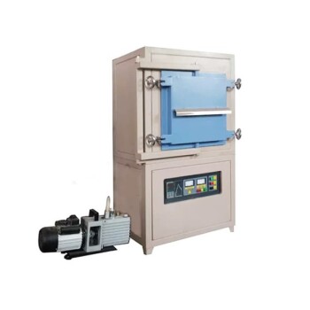
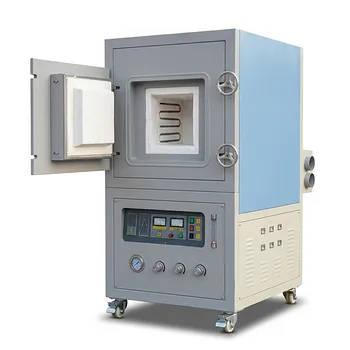
- 1700℃ Controlled Inert Nitrogen Atmosphere Furnace
- High Temperature Muffle Oven Furnace for Laboratory Debinding and Pre Sintering
- 1400℃ Controlled Inert Nitrogen Atmosphere Furnace
People Also Ask
- How does zone-melting in tube furnaces synthesize bismuth micro-wires? Master Single-Crystal Thermoelectric Growth
- How are high-temperature laboratory tube furnaces applied in long-term vacuum homogenization heat treatments for intermetallic samples?
- How are high-temp tube furnaces used to measure diffusion coefficients per Fick's law? Master Precision Annealing
- How do high-temperature laboratory tube furnaces ensure environmental stability? Precision Thermal Reduction Tips
- How are high-temperature tube furnaces applied in testing ceramic-supported alloy membranes? Insights